Abstract: A video compression system based on TMS320DM6446 is designed. The main chip uses TI's TMS320DM6446, and the analog video signal is sent to the decoder TVP5150, which is decoded to conform to ITU-R BT. 656 standard digital video signal, BT. 656 digital video signal is sent to TMS320DM6446, TMS320DM6446 embedded DSP to achieve video signal H. 264 compression, embedded ARM to package the compressed data and network transmission. Practice has proved that the coding scheme has done a good job of data compression and transmission. When the code rate is 372 kb/s, the PSNR is 39.18 dB (using the NEWS sequence), which meets the design requirements. This article refers to the address: http://
Light emitting diode (LED) light therapy is growing in popularity in both aesthetician offices and at home. Using varying LED wavelengths, this skincare technique purportedly helps treat acne, reduce inflammation, and promote anti-aging effects.
You may be a candidate for LED light therapy if you have these types of skincare concerns and haven`t gotten the results you want from over-the-counter (OTC) skin products. LED therapy is also safe for all skin colors, and it doesn`t cause any burning.
But there are a few catches. For one, LED therapy can be expensive, and the results aren`t guaranteed. It`s also not safe if you take certain medications or have an active skin disorder.
Talk to your dermatologist about your skincare concerns and whether LED light therapy is a viable option for you.
therapy lamp, light therapy lamp, phototherapy light Shenzhen Ri Yue Guang Hua Technology Co., Ltd. , https://www.ledlightinside.com
Keywords: video compression; embedded; DM6446; hardware design
With the development of multimedia technology, video surveillance systems are widely used in the security monitoring of road traffic, power systems, banks, hotels, shopping malls, communities, airports and other fields. The TMS3 20DM6446 chip is an outstanding representative of DaVinei technology. The TMS320DM6446 consists of TMS320C64x+DSP core, ARM926EJ-S core, video processing subsystem (VPSS), system control, power management, external memory interface, peripheral control module and other functions. Module composition, single TMS320DM6446 (hereinafter referred to as DM6446) can achieve H in full D1 format. 264 video compression.
This paper discusses the complete design of the embedded video encoder and completes the hardware design of a minimum video coding system based on DM6446.
1 Overall design and overview The system includes a power supply section, a video input section, a storage section, and an interface section. Its main resources include: DM6446 main processor; 2 CVBS standard analog video input (TVP5150); 256 MB DDR2 SDRAM; 64 MB NANDFlash memory; 1 RS485 serial port (MAX485); 1 10 M/100M standard Ethernet interface (RTL8201) ); 1 USB2.0 interface. The block diagram of the video encoder system is shown in Figure 1. 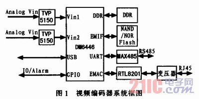
The system is mainly composed of the following two parts:
1) The video front end design analog video signal is input to the video decoding chip TVP5150. The TVP5150 inputs the decoded video data to the VPFE video port of the DM6446, and the DM6446 built-in DSP compresses the input data.
2) Network transmission and control part design DM6446 internal integrated Ethernet media access controller, external Ethernet PHY can provide Ethernet transmission channel. The DM6446 on-chip ARM9 microprocessor packs the compressed data and completes the network transmission. This section has a RS485 serial port for controlling external devices (pTZ controllers, etc.).
The DM6446 is a dual-core architecture. In the DM6446, the communication between the ARM core and the DSP core is mainly realized by interrupt. The DSP completes the data acquisition compression processing, etc. The role of the ARM processor is to configure and control the entire system, including: DSP subsystem, VPSS subsystem, most peripherals and off-chip memory, and TCP for compressed data. /IP package and network transmission, in addition to system resource scheduling and control of external devices (pTZ lens, etc.).
System workflow: After the system is powered on or reset, the program is loaded from the flash memory according to the configuration mode, and the initialization of the chip and the initial configuration of the peripheral device are completed. After the analog video signal is converted into the BT656 digital video signal by the TVP5150, the DM6446 is transmitted to the DM6446. The video channel (VFPE), after the embedded DSP encodes and compresses the digital video signal, the embedded ARM packs the compressed data and transmits it through the network interface.
2 module design
2.1 Video input part The system selects a high performance video decoding chip TVP5150 to convert the analog CVBS video signal to BT. 656 digital video signal, two TVP5150 are connected to the video input. The TVP51 50 clock source is a 14.318 18 MHz crystal, the digital and analog input voltage is 1.8 V, and the IO port voltage is 3.3 V. The PCLK/SCLK pin clock signal can output both 13.5 MHz and 27 MHz frequencies. After the analog signal is clamped by TVP5150, anti-aliasing filter, A/D conversion, it is configured to output YUV422 BT from YOUT[0:7]. The data stream of the 656 video format is input to the VPFE of the DM6446. The VPFE is composed of a CCD controller, a Preview engine unit, an H3A, a Resizer unit, and a columnar statistical function unit, and performs front-end processing on the input video data. VPFE is configured as a data format for YUV.
2.2 Storage Section In the DM6446, there are several forms of external memory interface. The DDR2 memory controller is connected to DDR2 SDRAM. The system uses two 16-bit MT47H64M16BT in parallel, and the storage space reaches 256 MB, which provides buffer for the system. After the VPFE processing, the data outputted to the DDR occupies a length of 16 bits per pixel at the time of storage, and each pixel occupies 2 bytes, and is continuously stored in the memory unit. If the pixel has a bit width of less than 16 bits, The extra high bits will be filled with 0s. DDR2 memory is used for system operation code, temporary movement of image data, and intermediate data for compression processing. The system maps 64 MB of NANDFlash in the CS2 memory space for storing the Linux kernel operating system and kernel bootloader.
2.3 Interface Section The system communicates with the peripheral communication interface module RS-485 through the serial port transceiver MAX485, which is used to control external devices (such as PTZ lens control).
The system contains 1 10/100 M network interface, DM6446 with MAC controller, 1 Ethernet PHY chip externally on EMAC interface, PHY adopts RTL8201, RTL8201 is connected with MII interface of DM365, DM6446 realizes RTL8201 register through MDIO interface Configuration and control, other handshake signals are connected in turn, and the RTL8201 is properly configured by the pull-up resistor (setting the PHY address, etc.), and the RTL8201 imports these configuration information at the beginning of power-on and performs corresponding work. A 25 M crystal is connected to the clock interface of the RTL8201 as the clock source for the RTL8201. The RTL8201 is connected to a network transformer for signal isolation and is connected to the network through RJ45 to exchange data with the outside world.
The DM6446 integrates a USB controller on the chip, which can operate the control memory map register through the ARM terminal. Many USB devices can be connected through the USB interface, and a peripheral expansion port is reserved for the system to implement additional functions.
The system provides 2-way switch alarm input and 2-way switch alarm output through GPIO. The alarm input is realized by the isolation diaphragm. When there is an alarm signal input signal, the diaphragm is turned on, and the output is low to DM6446 GPIO. When there is no alarm signal input, the diaphragm is cut off, and the output is high to DM6446 GPIO, DM6446. The presence or absence of the alarm input signal is judged by detecting the GPIO level. The alarm output is achieved by controlling the opening and closing of the relay.
2.4 Power Module The system power supply is divided into +5, +3.3, +1.8+1.2 V, and the input power is +5 V. The rest of the voltage is converted from +5 V power. Among them, +1.2 V provides DM6446 core voltage, +1.8 V for DM6446 I/O and DDR2 memory, and +3.3 V supplies power to most peripherals. The +1.2 V core voltage and the +3.3 V peripheral supply voltage are derived from the TPS75003, and the TPS62040 provides a +1.8 V voltage output. This design uses the MAX706 to reset the system.
3 Conclusion The system has been scientifically tested by the ITU-T video test sequence NEWS (150 frames). The test environment: one Panasonic notebook (with Intelpentium processor 1.1 GHz, 1 G memory, operating system Windows XP, 80 G hard disk) ). When the code rate is 372 kb/s, the PSNR is 39.18 dB, and the coding efficiency is reasonable, which is in line with the original intention of the design.
This paper effectively designs the embedded video processing minimum system by using DM6446, which fully meets the functional requirements of video compression coding. The system runs on the Linux operating system and has the characteristics of good real-time performance, fast communication speed, high image quality, stable performance, low price and anti-virus.