Die casting Zinc Alloy, Aluminum alloy and High Temperature powder coating are applied, which can effectively protect mechanical force and avoid water and powder, provide reliable protection for connected system against severe environment.
Four functions of heavy-duty connector housing:
1. Electrical insulation between connectors to avoid interference between signals.
2. Fixing the position of the connector is conducive to plugging and position stability.
3. Provide mechanical protection and support for the insert
4. Separate the connector from the application environment, reduce the environmental pollution and corrosion of the connector, and extend the service life of the connector
Hood Houses,Connector Hood,Connector Housings,Heavy Duty Connector Housings Suzhou WeBest Electronics Technology Co.Ltd , https://www.webestet.com
This article was also published in Maxim Engineering Journal, Issue 61 (PDF, 1MB).
A similar article was published in Electronic Products in October 2007.
More and more portable devices, such as digital cameras, cellular phones and portable media players, are gradually increasing the connection function of composite video output. In this type of device, a video filter amplifier connected behind a video digital-to-analog converter (DAC) generates a video signal. When the existing 3.3V video filter amplifier processes video signals, the power consumption is 45mW, which consumes a large amount of battery power.
Battery life is the key to portable devices, and any system IC that can extend battery life is of great significance. This will make the handheld device more attractive to users, because the device does not need to be frequently charged, so the user's use is more convenient. Extending battery life also means reducing the number of used batteries and the number of times the rechargeable battery grid is used. Both of the above two points are conducive to environmental protection. Maxim's next-generation video filter amplifier uses a 1.8V power supply and consumes only 12mW. Compared with the current 3.3V video filter amplifier, power consumption is reduced by nearly 70%.
Where is the energy consumption? Simply put, the power consumption of each circuit includes the loss of its own work and the loss of driving the load. In Figure 1, the power supply provides total current (IT) for the circuit, where IQ is the quiescent current of the op amp and IL is the load current. 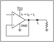
Figure 1. Single-supply operational amplifier with a resistive load to ground.
The power is obtained by multiplying the current and the power supply voltage. First calculate the static power consumption (PQ), load power consumption (PL) and total power consumption (PT) according to the following formula:
PQ = VDD × IQ
PL = VDD × IL
PT = PQ + PL = VDD × (IQ + IL)
In order to reduce the actual power consumed, both PQ and PL must be reduced. Reducing VDD, IQ and IL can achieve this goal.
Normally, IC data sheets will give IQ or PQ parameters, but rarely mention the average power consumption under typical signal and typical load conditions. For portable video filter amplifiers, PQ is almost useless information because the circuit is either off or fully on. When fully turned on, the video filter amplifier provides the video signal drive for the load. When there is no video load, in order to save battery energy, the video filter amplifier should be turned off; if the video filter amplifier is turned on when there is no video load, it will cause a waste of battery energy.
Power consumption of 3.3V video filter amplifier When the 3.3V video filter amplifier provides video signal drive to the load, the power consumption increases, as shown in Table 1. The average power consumption is defined as the power consumption when the video filter amplifier drives a 150Ω load to ground with a 50% flat-field video signal. As a typical video signal, a 50% flat field signal is displayed as a gray screen on the TV (PL depends on the image content, the power consumption is the lowest when the screen is black, and the power consumption is the largest when the screen is white). It should be noted in Table 1 that although the PQ of the components varies greatly, the average power consumption is very close.
Table 1. Average power consumption and static power consumption of various video filter amplifiers Company Part Supply
Voltage (V) Average
Current
(mA) Average
Power
(mW) IQ (mA) PQ (mW) Output Style Maxim MAX9502 3.3 13.5 44.6 5.3 17.5 PosiTIve DC bias TI® OPA360 3.3 12.2 40.1 6 19.8 Zero DC bias Maxim MAX9503 3.3 13.2 43.4 12 39.6 DirectDrive®
Driving the video signal to the video load causes increased power consumption, which depends largely on the output mode of the video amplifier. The MAX9502 uses a forward DC bias to output the video signal (see Figure 2). Maintaining the forward DC bias of the output signal increases the total power consumption. Therefore, the MAX9502 must supply approximately 8.7mA (the voltage indicated by the thick blue line in Figure 2b divided by 150Ω). 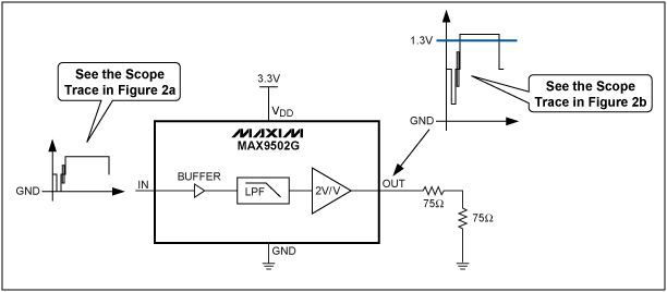
Figure 2. MAX9502G application circuit. The input and output are 50% flat-field signals. 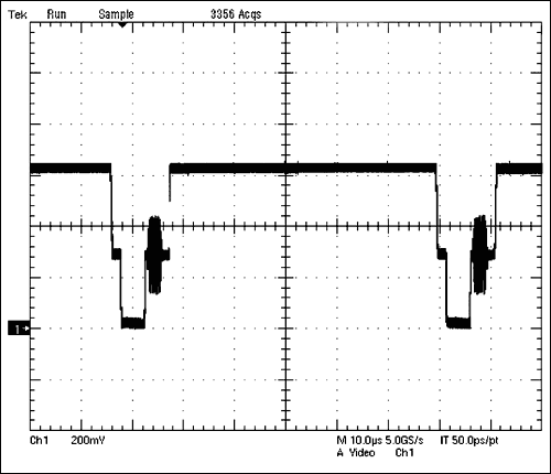
Figure 2a. 50% flat field signal waveform, input to the video filter amplifier to be tested. 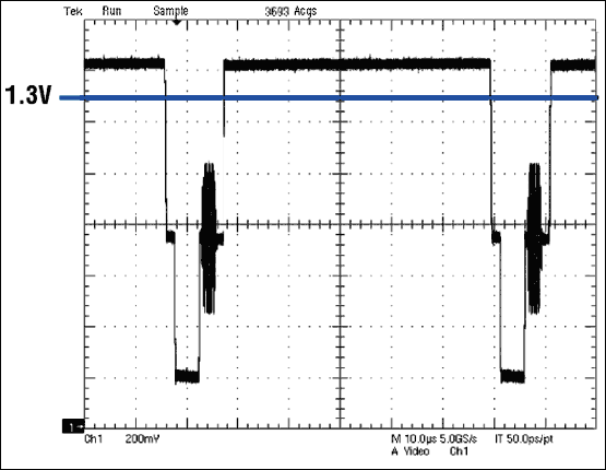
Figure 2b. The output waveform of the MAX9502G. The blue line indicates the approximate average DC level of the 50% flat field signal.
The output of OPA360 (Table 1) can work with the SAG network, which consists of two AC coupling capacitors (Figure 3). These capacitors block the DC connection between the output and the load. Therefore, the amplifier does not need to source or sink current to maintain the output bias, thereby reducing power consumption. 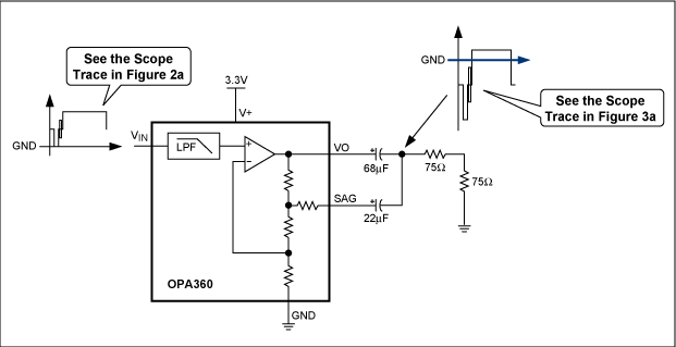
Figure 3. For a 50% flat field signal, because the capacitor blocks the DC connection between the output and the load, the OPA360 application circuit can effectively reduce power consumption. 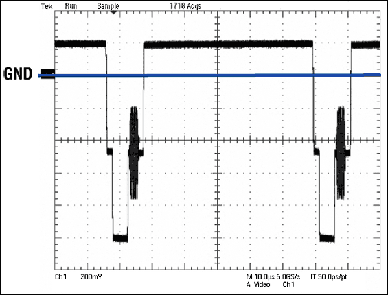
Figure 3a. The blue line in the OPA360 output waveform represents the approximate average DC level of the 50% flat field signal.
Using Maxim's patented DirectDrive technology *, the MAX9503 can output video signals with near zero DC bias without any AC coupling capacitors (see Figure 4). Because the on-chip reverse charge pump can generate negative voltages, this technology enables the MAX9503 to output signals below ground level. Although DirectDrive increases PQ, due to PL reduction, the average power consumption of the MAX9503 can be kept at the same level as the MAX9502 and OPA360. Because the DC bias is close to ground, the MAX9503 only needs to source a small current. 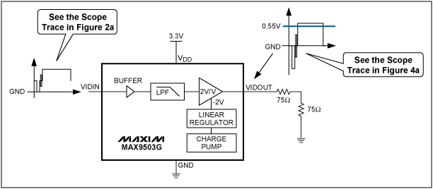
Figure 4. 50% flat field signal through the MAX9503G application circuit. 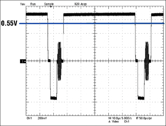
Figure 4a. The blue line in the MAX9503G output waveform represents the approximate DC average of a 50% flat-field signal.
Power consumption of a new generation of products: The MAX9509 1.8V video filter amplifier is the first device in Maxim's new generation of video filter amplifier series, which greatly reduces the average power consumption and PQ, as shown in Figure 5. The power supply voltage (VDD) has dropped from 3.3V to 1.8V, which is the digital I / O voltage that mobile phones are gradually using; the static power supply current (IQ) has also dropped from 12mA to 3.1mA (see Table 2). 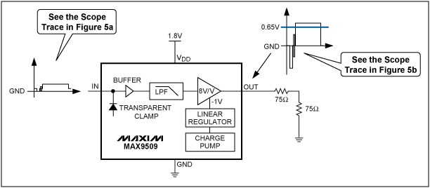
Figure 5. The MAX9509 1.8V application circuit processes 50% flat-field signals, greatly reducing power consumption. 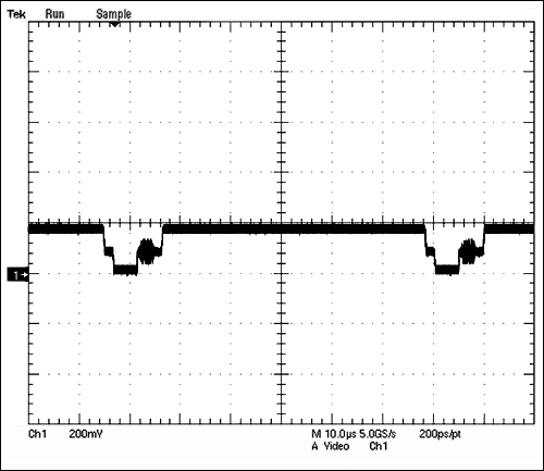
Figure 5a. The 50% flat field waveform is input to the MAX9509; its amplitude is one-quarter of the waveform amplitude in Figure 2a. 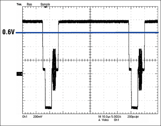
Figure 5b. The blue line in the MAX9509 output waveform represents the approximate DC average of a 50% flat-field signal.
Table 2. MAX9509 average power consumption and static power consumption Company Part Supply
Voltage (V) Average
Current
(mA) Average
Power
(mW) IQ (mA) PQ (mW) Output Style Maxim MAX9509 1.8 6.5 11.7 3.1 6 DirectDrive
Appendix Circuit Considerations for 1.8V Video Filter Amplifier gives specific issues that need to be resolved when designing a video circuit using a new 1.8V digital I / O voltage.
When the video filter amplifier works with 1.8V power supply voltage, DirectDrive technology must be used. Amplifiers using a voltage-mode output stage must provide at least 2VP-P swing to output a composite video signal. When the traditional amplifier is powered by a single 1.8V power supply, there is not enough margin to generate the 2VP-P output signal. After using DirectDrive, the integrated reverse charge pump will generate a noisy -1.8V voltage; the negative voltage linear regulator will stabilize the -1.8V voltage to -1V, reducing the charge pump noise. Therefore, due to the use of -1V to + 1.8V voltage supply, MAX9509 just has enough margin to output 2VP-P video signal.
The MAX9509 uses a low-voltage, low-IQ DirectDrive output stage. The average power consumption of the device (Table 2) is much lower than the power consumption of the 3.3V device in Table 1. This means that if the same battery is used to power the system containing the MAX9509 and the system containing the 3.3V device, the battery power required by the MAX9509 amplifier is 70% lower than that of another system, thereby extending battery life. This has a direct impact on the environment because it reduces the number of used batteries and rechargeable battery grids.
More notably, the average power consumption of the MAX9509 is lower than the PQ of a 3.3V video filter amplifier. It should be noted that at such a low voltage, the circuit works at high speed, the noise will increase greatly, because the working current of the circuit is lower than normal at this time. The MAX9509 considers noise issues during the design process. The device has an excellent peak signal-to-noise ratio (SNR) of 64dB, which is sufficient to meet the requirements of consumer products. In order to make the TV screen display a clear image, the peak SNR should be around 40dB.
Putting the noise-filled charge pump on the same chip as the filter and amplifier is the main design difficulty. The charge pump may introduce switching noise into the sensitive video signal. Isolating the MAX9509's charge pump from the video signal path can effectively solve this problem, resulting in extremely low charge pump noise frequency domain characteristics (Figure 6), and almost no noise is observed from the time domain characteristics (Figure 7). 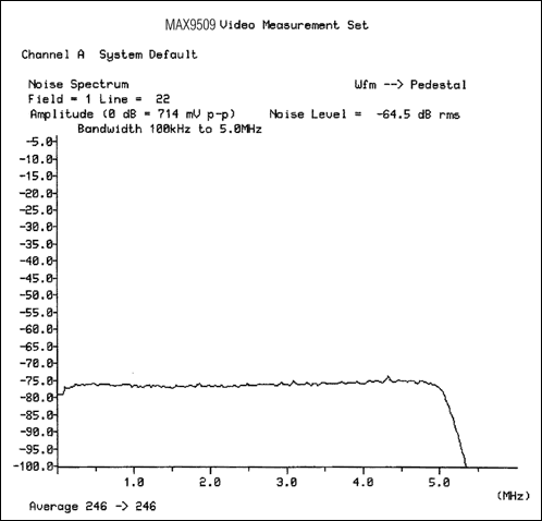
Figure 6. When measuring the noise and frequency relationship of the MAX9509, the noise spectrum of the charge pump is very small. 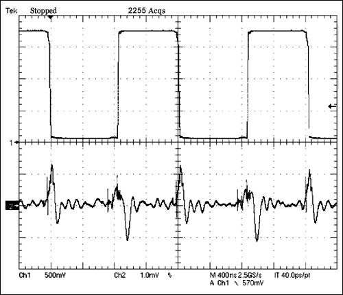
Figure 7. When the video signal is 1VP-P, the MAX9509 output changes over time (bottom graph), and the peak value is 1.4mVP-P. The top graph is the voltage of the charge pump flying capacitor.
When consumers observe the output signal of the MAX9509 on the screen, they will neither see broadband noise nor charge pump noise.
Development direction of low-power video filter amplifiers Although the development of low-power video filter amplifiers has made some progress, IC designers still have a lot of work to do. For example, video load detection. If the video filter amplifier has a load electronic detection function and provides the load status for the microcontroller system, only when the effective video load occurs, the video output circuit is turned on, which can further enhance the system's intelligent video power management. At present, most of the insertion of video load is detected through a mechanical jack to turn on the video output circuit. If the other end of the cable is not connected to a TV or other monitor, this method will cause a waste of battery energy. Another benefit of video load electronic detection is that only standard connectors are required, and no connectors with mechanical jack detection are required. Compared with standard connectors, this mechanical connector increases cost and takes up more space.
In portable devices, low power consumption has always been a top priority; considering the increasing energy costs and global warming, devices powered by wall adapters are also increasingly focusing on power consumption. Therefore, the development trend is to integrate more intelligent power management circuits in analog chips. For the video filter amplifier, not only should the power consumption be low, but it should also have video load detection, video input detection and control circuits in order to control the corresponding operating mode. Because video chips are generally used in consumer electronics products with fierce price competition, the biggest problem is how to enhance intelligent power management without increasing costs too much.
Appendix: Circuits of 1.8V video filter amplifiers. In considering product design, companies around the world, in addition to considering reducing costs and increasing functionality, are paying more and more attention to their environmental performance. Selecting low-power consumption and adopting lead-free / RoHS-compliant IC devices is the key to designing an environmentally friendly system.
When designing the MAX9509 low-power video filter amplifier, some special factors need to be considered. Setting the bias current to distribute the power supply current reasonably is the most effective way. Careful layout can reduce parasitic capacitance and achieve good device matching. Finally, we must carefully check and analyze the current of all branches in the circuit. This series of measures helps to reduce power consumption and reduce the bandwidth requirements of the circuit, only to meet the bandwidth requirements of frequency response and video performance.
Through careful circuit design and relying on Maxim's advanced BiCMOS process, the power consumption of the MAX9509 is much lower than that of the previous generation video filter amplifier. In order to achieve the lowest power consumption while meeting specific application performance requirements, we analyzed all previous-generation video design circuits. For example, reduce the mirror image of the bias current between the MAX9509 power supplies; use as little negative power as possible. In addition, a proprietary circuit is used to eliminate the distortion when the amplifier is operating at low current. Maxim's advanced analog process can optimize components for specific video signal channels (for example, bipolar and MOS), thereby further reducing the power consumption of the MAX9509. The MAX9509's 5-pole filter eliminates the biquad filter required by the previous-generation 6-pole filter amplifier (Figures 8 and 9). For consumer applications, the filtering performance of the 5-pole and 6-pole filters is not much different, and the elimination of the biquad filter will reduce the total supply current by more than 10%. 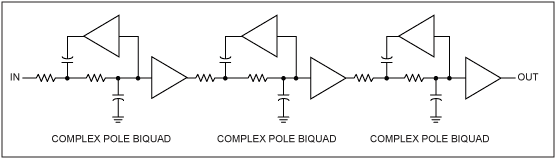
Figure 8. The previous-generation video filter amplifier used a 6-pole filter. 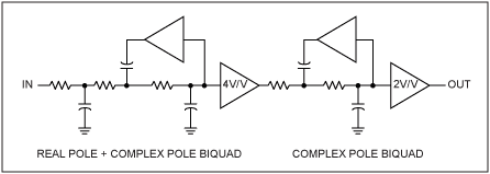
Figure 9. The MAX9509 uses only a 5-pole filter, eliminating the need for biquad filters, and reducing the total supply current by 10%.
By carefully placing the filter circuit and the amplifier circuit, each module of the signal channel is optimized under the given system parameters, thereby reducing the total current. For example, when the MAX9509 wants to obtain an 8-fold gain, a pre-amplifier with a 4-fold gain is used inside the filter. Therefore, the resulting video amplifier only requires a gain of 2V / V (Figure 9), thereby reducing the requirements for the final stage video amplifier and reducing power consumption. At the same time, the total power consumption of the two amplifiers is reduced to achieve the best performance.
Next-generation video filter amplifier extends battery life of handheld video systems
Abstract: More and more portable devices, such as digital cameras, cellular phones and portable media players, are gradually increasing the connection function of composite video output. In this type of device, the video digital-to-analog converter (DAC) generates a composite video signal that must be video filtered and amplified before being sent to the output connector. Design engineers have considered power consumption, overall cost, size, and image quality when selecting video filters. This article focuses on how the next-generation video filter amplifier can extend battery life and other needs in next-generation portable devices.