Altera is a registered trademark of Altera Corporation.
LED Switches
LED Switches, belong to Led Light Switches serious, is also called flat-reset LED indication switch. The overall appearance of the product is a flat panel type, and can be automatically reset. The switch function part has an LED indicator, which not only accurately indicates the on/off state of the switch, but also makes it easy for the user to find the switch position in the darkness.
LED Push Button Switches are suitable for consumer products, computer products, test instruments, communication equipment. This light switch could contain momentary switches and self lock and it is very sensitive. It could work only with a little strength, just a bit like Micro Switches . Furthermore, the shape of the light could be round, square and five position as well. In addition, we could equip with all kinds of color for the LED On Off Switch, including white,yellow,red, green,etc. One more important advantage for our light switch is that we could equip with double color for the LED Light switches,like red&green, red&blue, red&yellow.
Different from other switches,including Metal Switches , Rotary Switches, Slide Switches , Automotive Switches, LED switches is a flat design with no rocker protruding parts. The style is modern and fashionable,not easy to dust. Its opening and closing operations are all in the same position. After the release of the hand, the rocker automatically restores the flatness and feels better and lasts longer.
LED Switches Led Light Switches,Led Light Switch 220V,Led Light Dimmer Switch,Lighting Switch With Led Indicator YESWITCH ELECTRONICS CO., LTD. , https://www.yeswitches.com
Introduc TIon Roughly tens of thousands of large-size LED video-display boards have been installed worldwide. The adopTIon of LED video display boards can become even more widespread if the overall system price can be significantly reduced and the operaTIonal procedure of such display boards can be simplified . The following application note represents a reference design for a basic, low-cost, modular LED video-display board. The design's new architecture uses a combination of one inexpensive FPGA chip for the digital video bit stream demultiplexing and the features of MAX6974 LED drivers to build a QVGA (320 x 240) resolution LED video display. This display board can be controlled by a PC and used as a secondary monitor to display any text, graphic, or multimedia information.
Current LED Video-Display Board ArchitectureCurrently, all of the top LED video-display board manufacturers have similar but proprietary architectures using LED video bricks of different color pixel sizes. The video-brick pixel size ranges from 256 to 15552, depending on the manufacturer. The video bricks can be put next to each other to assemble a video wall of a few meters in size on each side (Figure 1). LEDs and their drivers are mounted close to each other on different PCBs inside each video brick. Also included on the LED-driver PCB are an FPGA and video-buffer memory chips.
For a video wall, interconnections between video bricks are normally made using coaxial cables. The video wall is then linked to control and video processing units by optical fiber. The control unit is used to configure these video bricks and select the proper video source. The video processor receives the selected video signal, converts its format, and sends the correct data information to the corresponding pixel position. Data buffering and scaling are also tasks completed by the video processor. The application's controller and video processor units are specialized professional equipment that can be very expensive. 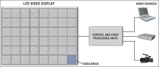
Figure 1. Today's LED video-display board system architecture.
Maxim's ApproachUsing the unique features of the MAX6974 LED driver, an LED video-display board can be constructed with the help of a low-cost, medium-size FPGA chip. The entire system is controlled by a PC (Figure 2). With the addition of a video-interface PC card, different video-signal sources can all be accommodated. The result is a complete LED video-display board with fewer electronics components and no need for specialized operational equipment. 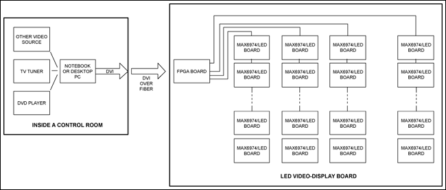
More detailed image (PDF, 12kB)
Figure 2. MAX6974-based LED video-display board system architecture.
The MAX6974 LED Driver FeaturesThe MAX6974 LED driver is designed specifically for LED video-display board applications. Each LED driver has 24 coordinated, constant-current, PWM LED driver ports and can drive eight or 16 (duplex mode) RGB pixels. To accommodate video or still camera pictures without the outcome being a blank screen, the PWM rate of this chip is very fast. At a video refresh rate of 60fps (frames per second), the PWM rate is about 7680Hz. The MAX6974's data-input interface consists of one LVDS clock and LVDS data pairs. Data bits intended for additional serialized MAX6974 LED drivers are available through a data-output interface, which also includes an LVDS clock and a LVDS data pairs. Depending on the video refresh rate and the clock frequency, hundreds of MAX6974 devices can be linked together through the LVDS interface. Because of this interface, interconnections between the LED drivers and the video-display module PCBs can be made through twisted-pair cables of up to a few feet.
The intensity of each LED can be controlled in three ways by the MAX6974. First, each individual LED (red, green, or blue) has a PWM intensity control of 12 bits. That is much more than the 8-bit per color resolution defined by the DVI â„¢ interface. The extra bits may be used for contrast adjustments to accommodate different ambient lighting conditions. Secondly, there are 7 bits of PDM intensity control affecting all LED drive ports. These PDM bits can be used for brightness control. Last, there are 256 (6mA to 30mA) steps of constant-current control for each color group of LED drive ports. These calibration steps can be used to match the desired video color temperature.
Detailing a MAX6974-Based LED Video-Display Board ArchitectureThis LED video-display board reference design uses a single FPGA chip to demultiplex video data bits. It also captures control frames and directly forwards them into corresponding registers inside each MAX6974 LED driver. Figure 3 shows the functional block diagram of this reference design with QVGA resolution (320 x 240) using a TFP401A DVI receiver, an AT24C02 EEPROM to store an EDID, an EP2C20 FPGA, and 9600 MAX6974 LED drivers to drive 76,800 OVSRRGBCC3 RGB LEDs. 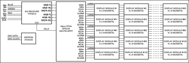
More detailed image (PDF, 68kB)
Figure 3. Reference design functional block diagram.
The DVI signal on the left side of the block diagram is received by the TFP401A DVI receiver. The AT24C02 EEPROM is used to provide an EDID for the Windows® operating system. The deserialized and TMDS-decoded signal is then sent to the EP2C20. Reformatted video bits are made available to columns of the LED display module PCBs through 5 LVDS channels at a speed of about 32Mbps. An LVDS channel consists of 2 differential pairs, CLKI (O) ±, DIN (OUT) ±, a LOADI (O) pin, and a GND (ground) pin, for a total of 6 wires. Each LED display module PCB contains 64 MAX6974 LED drivers and 512 OVSRRGBCC3 RGB LEDs.
Video Bit Stream Demultiplexing and Control Video FrameThe lowest resolution for DVI is VGA. For the QVGA application of this reference design, only odd or even pixels and every other line are used. The half pixel clock rate from the TFP401A DVI receiver is 12.5MHz. The blanking overhead is approximately 40%. By taking only odd or even lines and purging the blanking overhead that is not required for the MAX6974's LVDS interface, the serialized (24-bit RGB) QVGA data rate is 12.5 / 2 / 1.4 × 24 = 107.142857Mbps. The effective data rate, considering DVI's 8-bit per color conversion to the MAX6974's 12-bit per color conversion, is 107.142857 / 8 × 12 = 160.714286Mbps. The FPGA buffers the pixel data stream from the TFP401A DVI receiver, separates it into five groups, and sends them to their corresponding LVDS channels. The data rate at each LVDS channel is 160.714286 / 5 = 32.1428571Mbps.
Each pixel is delivered in sequence from left to right on each line and from the top to bottom on each frame through the TFP401A DVI receiver. The MAX6974's individual PWM frame format requires the same color information for a group of eight pixels to be delivered together ( Table 1). A buffer is needed to hold at least eight pixels of data for this format conversion. A buffer for the entire video frame is used for the reference design, taking into account the adjacent line and blanking overhead removal, while maintaining an almost constant data delivery rate through the LVDS channels. The buffering also enables the interconnection of multiple MAX6974 devices at both ends of a PCB, thus avoiding long LVDS links from right to left ends.
Table 1. MAX6974 Individual PWM Data Frame Format
B _... G _... R_ 12-bit (MAX6974) or 14-bit (MAX6975) data each HEADER DATA 1 DATA 2 DATA 3 ... DATA N HDR [23: 0] B7, B6, ... R0 B7, B6, ... R0 B7, B6, ... R0 ... B7 ... R0
Besides delivering the individual port PWM information, three other data frames with header CMD bits of 010101, 101010, and 111111 are used to deliver CALDAC, global intensity PDM, and configuration information through the MAX6974's LVDS interface (Table 2). Each header consists of 24 bits. The first byte is the same synchronization pattern of 11101000, followed by six CMD bits, and then ten counter (CNTR) bits. The CMD bits for the individual port PWM data frame is 000000.
Table 2. MAX6974 Data Frame Header Format HDR twenty three twenty two twenty one 20 19 18 17 16 15 14 13 12 11 10 9 8 7 6 5 4 3 2 1 0 SYNC CMD CNTR 7 6 5 4 3 2 1 0 1 0 1 0 1 0 9 8 7 6 5 4 3 2 1 0 1 1 1 0 1 0 0 0 C1 C0 C1 C0 C1 C0 b9 b8 b7 b6 b5 b4 b3 b2 b1 b0
Data frames, other than those containing PWM information, are also sent through the DVI interface utilizing a PC-based GUI. The data frame type is identified by corresponding circuits inside the FPGA. Data frames, other than those related to PWM information, have the format shown in Table 3, where HDR stands for header. Note that video frames for individual port PWM information do not contain a header.
Table 3. Video-Display Reference Design, Data-Frame Screen Format Row LVDS 1
Pixel 0 ~ 63 LVDS 2
Pixel 64 ~ 127 LVDS 3
Pixel 128 ~ 191 LVDS 4
Pixel 192 ~ 255 LVDS 5
Pixel 256 ~ 319 0 HDR ... HDR HDR ... HDR HDR ... HDR HDR ... HDR HDR ... HDR 1 HDR ... HDR HDR ... HDR HDR ... HDR HDR ... HDR HDR ... HDR 2 Chip 1 ... ... Chip 1 ... ... Chip 1 ... ... Chip 1 ... ... Chip 1 ... ... ... ... ... ... ... ... ... ... ... ... 31 .. Chip 1920 .. Chip 1920 .. Chip 1920 .. Chip 1920 .. Chip 1920 32 HDR ... HDR HDR ... HDR HDR ... HDR HDR ... HDR HDR ... HDR 33 HDR ... HDR HDR ... HDR HDR ... HDR HDR ... HDR HDR ... HDR 34 Chip 1 ... ... Chip 1 ... ... Chip 1 ... ... Chip 1 ... ... Chip 1 ... ... ... ... ... ... ... ... ... ... ... ... 63 .. Chip 1920 .. Chip 1920 .. Chip 1920 .. Chip 1920 .. Chip 1920 64 HDR ... HDR HDR ... HDR HDR ... HDR HDR ... HDR HDR ... HDR 65 HDR ... HDR HDR ... HDR HDR ... HDR HDR ... HDR HDR ... HDR 66 Chip 1 ... ... Chip 1 ... ... Chip 1 ... ... Chip 1 ... ... Chip 1 ... ... ... ... ... ... ... ... ... ... ... ... 95 .. Chip 1920 .. Chip 1920 .. Chip 1920 .. Chip 1920 .. Chip 1920
Table 3 represents a partial control video frame of 320 pixel columns and 96 pixel rows. LVDS channels 1 through 5 deliver video and control information for pixel columns 0 through 63, 64 through 127, 128 through 191, 192 through 255, and 256 through 319 respectively. In a control video frame, each pixel in rows 0 and 1 contains the 24 header (HDR) bits of the configuration. Rows 32 and 33 host the header bits of the global intensity PDM, and rows 64 and 65 contain the header bits of the CALDAC. The 30 rows that follow each group of 2 header rows correspond to 30 rows of LED display module PCBs of this reference design. The 64 pixels of each row within a particular LVDS column have the information for 64 MAX6974 LED drivers on each LED display module PCB. Each pixel contains the 24-bit control information for one MAX6974 device. Rows beyond 95 are not used in a control video frame.
GUI for Display Board ControlA GUI (Figure 4) is used to set up the configuration, global intensity PDM, and CALDAC register bits for all MAX6974 devices utilized in this design. On the GUI, there is a global setting option for adjusting corresponding parameters for all chips on a video-display board. There are also device tabs where parameters for each chip can be adjusted individually. Settings for all registers and all MAX6974 LED drivers can be saved to a file and loaded once the video-display board is turned on . There is an initial settings file with typical register parameters to simplify the video-display board product-initialization process. 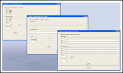
More detailed image (PDF, 588kB)
Figure 4. MAX6974 video-display board GUI.
The GUI appears in the Windows operating system as an individual application window. It creates a video control frame and sends it to the video-display board once the Write button on the GUI is activated. The video control frame only needs to appear once in a video refresh rate of 60Hz. The video control frame could occupy the entire screen of the of the video-display board; however, the FPGA detects the control frame header rows and sends corresponding information to MAX6974's registers directly. Therefore, the contents of video control frame will not appear on the video-display board. Although this skips a video-frame update, it is not noticeable to the human eye.
ImplementationsThe DVI receiver board contains one TFP401 DVI receiver and one AT24C02 EEPROM, plus a few bypass capacitors (Figure 5). The TFP401 DVI receiver performs the serial-to-parallel conversion and TMDS decoding, and it makes odd and even pixels of RGB bits available simultaneously at a half-pixel clock rate. Because the minimum screen resolution defined by DVI is VGA, this reference design purges every adjacent pixel and every other line. The half pixel clock is convenient for the FPGA, allowing it to pick and choose the desired pixel.
Before the Windows operating system recognizes a monitor, it probes the monitor through DDC using an I²C protocol. The monitor then responds with its EDID that contains manufacturing and operations information. Similarly, the AT24C02 EEPROM is used to store the EDID information for the LED video -display board. The manufacturer's ID must be obtained from the Video Electronics Standards Association (VESA). For this reference design, the EDID of a DVI-capable LCD monitor is borrowed and stored into the AT24C02 EEPROM. When all of its three address pins are grounded, the I²C device address of the AT24C02 EEPROM is 0xA0, which is what the operating system will be searching for. 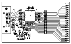
More detailed image (PDF, 160kB)
Figure 5. DVI receiver PCB (2.25 "x 4").
The FPGA board (Figure 6) consists mainly of two SRAMs, and a single Altera® FPGA device. Both LVDS interface and memory access functions reside inside the FPGA. The FPGA's main purpose in this design is the demultiplexing of DVI digital video information. Another important function of the FPGA is data-frame recognition for configuration, global intensity PDM, and CALDAC information. These data frames, containing other than the individual PWM information, are received and directly sent to the corresponding MAX6974 registers once a video control frame is identified . 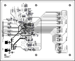
More detailed image (PDF, 304kB)
Figure 6. FPGA PCB (7.5 "x 9.5").
Figure 7 shows the internal functional blocks of the FPGA. A screen frame of the pixel bits is stored in the SRAMs for buffering. Line buffers implemented inside the FPGA are used to interface the TFP401A DVI receiver and the LVDS channels. Two line buffers, one for accepting data bits from the TFP401A DVI receiver and the other for transferring to the SRAM, are used to accept data from the TFP401A DVI receiver. Similarly, two line buffers are used for each LVDS channel. The FPGA provides combination logic circuits to meet the timing requirements for matching both DVI and LVDS data throughputs and for all necessary SRAM data, address, and control signals. Because the SRAM is a single-port type, while both Read and Write operations are carried out simultaneously, a memory-access-scheduling mechanism is also implemented inside the FPGA. 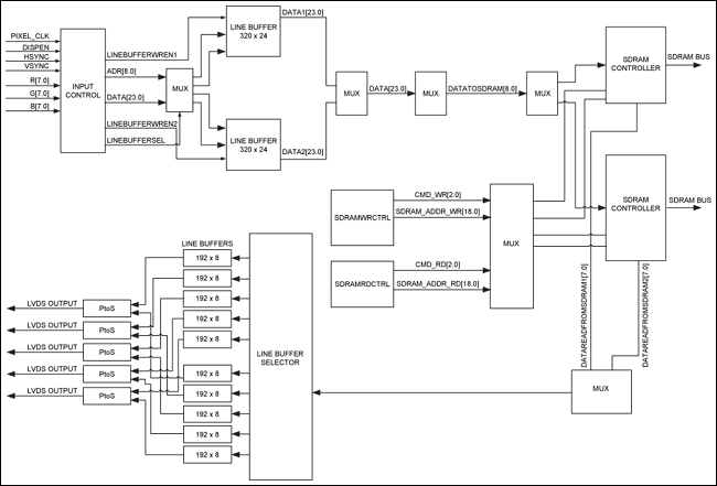
More detailed image (PDF, 56kB)
Figure 7. FPGA internal functional blocks.
Each MAX6974 drives eight RGB LEDs. Each display module board (Figure 8) contains 64 MAX6974 LED drivers in eight rows and eight columns, plus 512 RGB LEDs in eight rows and 64 columns. All LEDs are assembled on one side of the PCB with an LED center-to-center distance of 8mm from their top, bottom, left, and right neighbors. The dimensions of the display module board are 512mm x 64mm. All MAX6974 devices are assembled on the other side of the PCB. On the same side where MAX6974 devices are assembled, power and ground pins, as well as 1 x 6 headers, are also installed. Two 1 x 6 headers are installed: one for the LVDS input interface at the top left corner, and the other for the LVDS output interface at the bottom left corner. The display module board is designed to be snapped on to a display board frame where interconnection boards are installed. No additional wiring is required for the LVDS interface between adjacent LED display module PCBs. 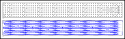
More detailed image (PDF, 1.25MB)
Figure 8. LED display module PCB (64mm x 512mm) with the LEDs assembled on one side and the MAX6974 LED drivers on the other side. (The PCB is broken into left (a) and right (b) sides.)
Figure 9 shows the general assembly of the QVGA LED video-display board with a DVI receiver, an FPGA, and 150 LED display module PCBs. These PCBs are arranged in 5 columns and 30 rows. DVI receiver and FPGA PCBs are shown on the top of the video-display board assembly. They can easily be hidden behind the LED display module PCBs in the top rows. 
More detailed image (PDF, 60kB)
Figure 9. Video-display board assembly.
Power ConsumptionThe operating current for each MAX6974 device is 28mA (CALDAC inactive) or 54mA (CALDAC active) from a 3.3V VCC supply. The operating current for 64 MAX6974 LED drivers on an LED display module PCB is 1.8A or 3.5A. The maximum LED current through each MAX6974 port is 30mA from a 5V VLED supply. The maximum LED current for each LED display module PCB with 512 RGB LEDs is 46A. Multiple 3.3V and 5V supplies are necessary to provide power for the entire video-display board.
An 80 x 64 LED Video Brick Figure 10 shows 9 LED PCBs assembled in an acrylic frame (capable of fitting 10 PCBs) with FPGA and DVI receiver PCBs mounted in the back (see Figure 11). The entire QVGA display board can be assembled using 15 (3 x 5) such acrylic frames. 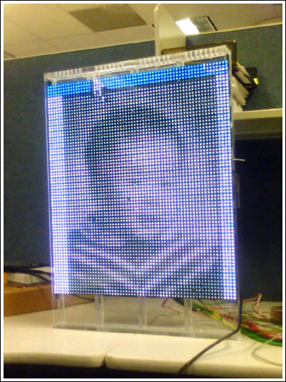
Figure 10. An acrylic frame that houses up to 10 LED PCBs. 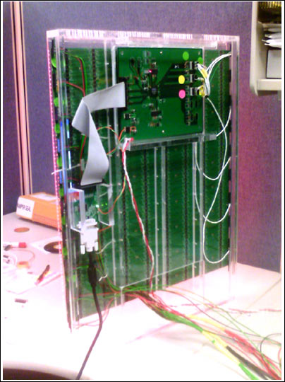
Figure 11. The back side of the acrylic frame.
DVI is a trademark of Digital Display Working Group (DDWG).
Windows is a registered trademark of Microsoft Corp.


Design an LED-based video display board-Designing an LE
Abstract: Currently, all of the top LED video-display board manufacturers have similar but proprietary architectures using LED video bricks of different color pixel sizes. Maxim has taken its knowledge of these applicaTIons and incorporated the unique features of the MAX6974 LED driver into a reference design for an LED-based video-display board that is used with a low-cost, medium-size FPGA chip.