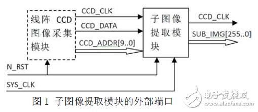
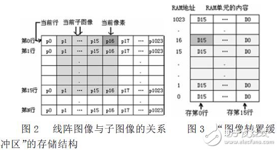
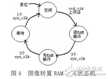
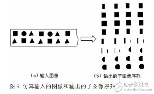
0 Preface In industrial production automation systems, product quality monitoring and control through computer vision and image processing technology has gradually become an effective application technology. Linear CCD image sensors are widely used in product size measurement and classification, non-contact size measurement, barcode, shape recognition and many other fields. In the image detection system, a high-speed sub-image extraction and output module should be provided. In this paper, the FPGA device EP3C25F256C8 and the CCD line image sensor RL1024P are used to realize the sub-image extraction and output functions in the line CCD image detection system. 1 sub-image extraction module design The function of the sub-image extraction module can be described as follows: using an FPGA device, the sub-images of the set size in the image are extracted according to the black-and-white image and the synchronization signal of the serial input. Suppose the input image size is i * j, the coordinate position of a pixel is (X, Y), and the size of the sub-image to be taken is m * n, which is described by c code as: for(b=0;b"j ; b++){for (a=0;a"i; a++){ // extract Xa, Yb to Xa+m, sub-image of Yb+n;} } According to the requirements of the system design, the line CCD image acquisition module outputs 1&TImes; a line of 1024 pixels in a serial manner, and the sub-image extraction module receives the image data, buffers, and outputs 16&TImes; 16-pixel sub-images. The external port of the sub-image extraction module is shown in Figure 1. The main signals are: pixel synchronous clock signal CCD_CLK, pixel data CCD_DATA, current input pixel coordinate CCD_ADDR[90]; in addition, N_RST and SYS_CLK are the reset signal and processing clock signal provided by the system. Among them, the CCD_DATA pixel is valid when the rising edge of each CCD_CLK appears, and the position of the pixel is CCD_ADDR[90]. In order to output a sub-image every CCD_CLK cycle, SYS_CLK should be about 10 times CCD_CLK. This paper uses the "image transposition buffer" method to implement the sub-image extraction module. The Image Transpose Buffer is a RAM buffer that is written (updated) by row and read out by column. A 1024-cell RAM buffer is set inside the FPGA. The bit width of each cell is 16 bits. The relationship between the line image output from the line CCD acquisition module and the sub-image is shown in Figure 2. The 0th line indicates the current line of the image, and the Nth line is the history line. Each line has 1024 pixels and is output in the order of pixels from p0 to p1023. Assuming that the pixel of the current CCD_CLK input is the p16 pixel of the 0th line, its corresponding 16X16 sub-image is the shaded part in the figure. The Image Transpose Buffer RAM block stores the structure of the image, as shown in Figure 3. The RAM block has a total of 1024 cells, each of which is 16 bits wide and holds the most recent 16 lines of image data. Comparing Figure 2 with Figure 3, it can be found that the address number of the RAM block is equivalent to the position of a row of pixels of the line CCD image. The bits D15 ~ D0 of a RAM unit correspond to the last 16 pixels of a column, which is equivalent to the line. The image is transposed and stored in the RAM block. When writing to the RAM buffer, since the data of the line CCD image is input bit by bit, when the rising edge of each CCD_CLK clock appears, only the bit corresponding to the current pixel in the RAM buffer needs to be updated, so logically It is written to the RAM area by line according to the image. In an FPGA device, a state machine can be designed to implement the read and write operations of the Image Transpose Buffer, as shown in Figure 4. The sub-image extraction module outputs a sub-image with 256 pixels, and temporarily stores an output sub-image through a register in the FPGA; when updating a pixel in the RAM area, the 16X16 sliding window is moved to the right by a column of pixels. By taking the data in the sliding window as an output, a new sub-image can be obtained. 2 design simulation In the design simulation of this paper, due to the use of image file analysis and image display, the joint simulation by means of MATLAB and Modelsim software can make the simulation process more convenient and intuitive. Among them, MATLAB is used to convert image files into input pixels and display sub-images of output; Modelsim is used to simulate and verify that the FPGA design is correct. This article uses MATLAB and Modelsim for co-simulation, the main three steps. The first step is to write the m file in MATLAB, read the bmp bitmap file and write the pixel data to the file datain.txt as the input stimulus for the ModelSim simulation. In the second step, in ModelSim, the Testbench test file is written in VHDL, the datain.txt file is read, and the pixel signal synchronized with CCD_CLK is generated. The DO file is written for automatic simulation, and the sub-image data of the simulation output is saved in dataout.txt. In the file. The third step is to write the m file in MATLAB, parse the dataout.txt file, and display the black and white image sequence of 16&TImes;16 in turn to determine whether the simulation result is correct. This design simulates the input image and the output sub-image sequence, as shown in Figure 5. From the simulation results, the design method is correct, and the simulation results meet the requirements of the design function. 3 Conclusion When using linear array CCD image sensor for product inspection, continuous and high-speed output of sub-image sequences is an indispensable important link. FPGA is used to extract and output sub-image sequences. There are many different design methods. In this paper, the image transposition buffer and state machine are used to realize the sub-image extraction and output functions required by the system. The design is jointly simulated by MATLAB and ModelSim tool software. Simple structure, high-speed processing, and convenient and intuitive features have a good reference for other similar FPGA design projects.
An electrical appliance used to protect electrical equipment from high transient overvoltage hazards and to limit the duration of continuous flow.This term includes any external clearance necessary for the normal functioning of the appliance during operation and installation, whether or not it is a unit as a whole.
Surge Protector, also known as lightning arrester, is an electronic device that provides safety protection for all kinds of electronic equipment, instruments and communication lines.When the electric circuit or communication lines or for outside disturbance suddenly produce peak current in voltage, surge protector in a very short time conduction tap, to avoid surge damage to other devices in the circuits.[1]
Surge protector, suitable for ac 50/60 hz, rated voltage 220 v to 380 v power supply system, the indirect lightning and thunder and lightning directly affect transient over voltage surge protection, or other applicable to the family home, the third industry and the surge protection industry requirements.
Surge Protector,Surge Voltage Protector,Eco-Friendly Surge Protector,Lightning Protection Surge Protector YANGZHOU POSITIONING TECH CO., LTD , https://www.yzpstcc.com