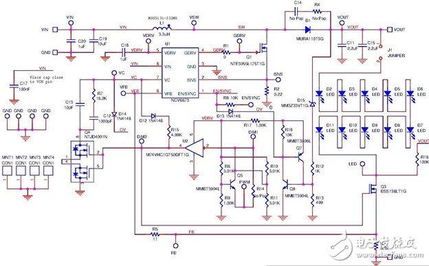
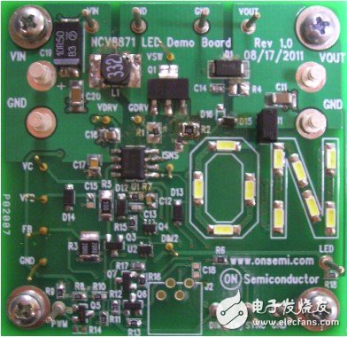
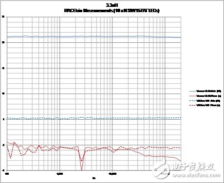
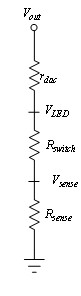
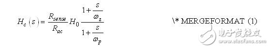
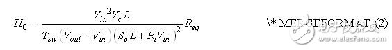
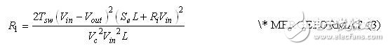
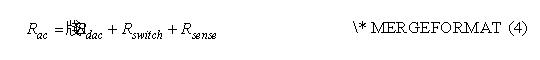
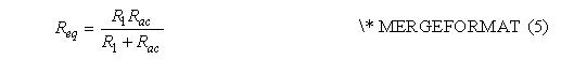
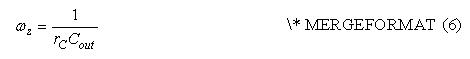
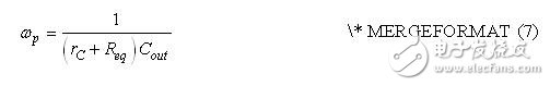
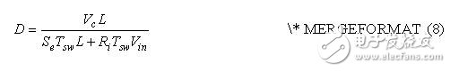
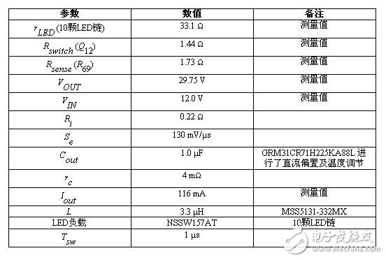
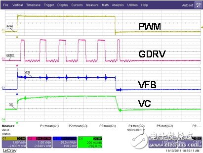
The first part of this paper is a theoretical analysis of the boost converter that drives the LED string. Inspiring this research is the need to stabilize the backlighting loops for automotive applications. Loop control is an important design consideration that affects final performance due to the application of pulse width modulation (PWM) for dimming control. The second part introduces the application scheme and compares the measured frequency response with the theoretical derivation value. LED dimming control system circuit diagram Analog dimming of high-brightness white LEDs produces color cast. PWM digital dimming control is the preferred dimming method to prevent color shift, because the luminous intensity will be the average lumen intensity. The LED current amplitude and the dimming ratio during the PWM on period are independent of each other. Figure 1 represents an automotive application LED dimming control system that consumes less than 10 μA of quiescent current in shutdown mode. It uses ON Semiconductor's NCV887300[1] 1 MHz non-synchronous boost controller, which operates in a constant frequency discontinuous peak current mode. The load consists of a series of 10 series Nichia NSSW157-AT[2] white high brightness LEDs. The corresponding circuit board is shown in Figure 2. Figure 1: LED PWM dimming control circuit using NCV887300. Figure 2: NCV887300 LED Demo Board. For ease of analysis, the key parameters of the NCV887300 controller are listed below: - When VIN = 13.2 V, the quiescent current (Iq) < 6 μA (-40 °C < TJ < 125 °C). - EN/SYNC pin: Can be connected to an external TTL command. Pins have dual functions and also support oscillator synchronization to an external clock - ISNS: The boost transistor current sense current limit threshold voltage is 400 mV; the internal slope compensation is 130 mV/μs. - VC: Internal Operation Transconductance Amplifier (OTA) compensation pin. There is a die-level 542 W ESD neutral protection resistor between the package pin and the amplifier output. The typical transconductance gm is 1.2 mS. OTA provides 100 μA 汲 current / source current capability. - VFB: LED current sense resistor R29 is regulated based on an internal reference voltage of approximately 200 mV. The design goal and working principle of the LED PWM dimming control circuit shown in Figure 1 are as follows. Design goals With a 6 to 18 V input voltage operating range, this circuit can support a 1000:1 PWM dimming ratio at 200 Hz PWM dimming frequency, resulting in a calculated minimum pulse width of 5 μs. The NCV887300 operating at 1 MHz produces a minimum of 5 boost transistor gate pulses to maintain the output capacitor charge supplied to the LED current. A discontinuous conduction mode (DCM) boost topology is required to maintain regulation because the boost inductor energy is fully released after each gate pulse. Continuous Conduction Mode (CCM) topologies result in poor regulation and undesired analog dimming because the boosted inductor's energy-enhanced inertia requires several duty cycles. Output leakage current losses must be minimized to help maintain output capacitor charge during deep dimming operation. The leakage current causes some output voltage discharge during the LED PWM off time, which in turn produces some analog dimming, which causes the compensation network to exhibit significant errors when the PWM is turned on. - Schottky rectifiers suffer from temperature-dependent large leakage currents. In order to minimize the boost rectifier leakage current, the ultra-fast technology boost rectifier was chosen in the circuit. - Ceramic capacitors have a much lower leakage current than electrolytic capacitors and are the preferred output boost capacitors. - The output overvoltage monitoring circuit current consumption must be kept to a minimum. A monitoring circuit that utilizes a grounded resistor divider network is not suitable. The Zener-excited overvoltage detection circuit is selected in this circuit because the Zener knee voltage is much higher than the battery voltage and the leakage current is extremely low. Circuit operation information Q18 blocks digital current for PWM digital dimming control. When the PWM instruction is active low, D34 clamps the IC's VFB feedback control voltage to a value below the controller regulation point and blocks the boost IC GDRV FET gate drive signal. Q15 is used as a compensation network status sampling/maintenance function for deep dimming applications. GM disconnects the compensation network during PWM dimming, feedback compensation capacitor charge (C31 and C32) is maintained, and fast dynamic control resumes when the PWM instruction becomes active high. Q14 is used with R48/R49/R51/R52 for level shifting of 1.8 V logic PWM dimming signals, and U7 buffers PWM signals to drive bidirectional switch Q15. If an LED open fault event is not detected, it will result in an overvoltage operating condition. The current sense resistor R29 voltage feedback will be 0 V, which will result in an open loop output overvoltage condition. Discrete passive components are selected in the circuit to apply overvoltage protection to minimize output leakage current losses when the LED system is externally turned off. The D31 Zener diode senses the overvoltage condition and initiates a soft start (D29) of the controller IC by pulling the enable pin low and interrupting the boost switch operation (D28). Resistor R30 provides a discharge path for output boost energy storage capacitor C22. Removing jumper J1 will turn off the LED chain to support an external load connected between the VOUT terminal and the LED terminal. Resistor R44 is the signal injection point of the frequency response analyzer at the VFB and FB terminals. Its presence does not affect the system loop response. By injecting a frequency response analyzer signal across R44, it is possible to measure the open loop gain (FB/VFB) response in the control output (FB/VC terminal), amplifier (VC/VFB), and closed loop form. LED AC dynamic impedance characterization The LED dynamic impedance can be approximated based on the characteristic curve measured under specific operating conditions in the manufacturer's data sheet. The specific thermal operating conditions of the system may vary widely. The system-level method of system LED dynamic impedance is described in the first part of the article. This method performs characterization of the device under system-level thermal conditions. For the second part of the article, we use a frequency response analyzer to measure the current sense resistor, PWM FET impedance, and cumulative series dynamic impedance in a circuit under 100% PWM duty cycle thermal stability (see Figure 3). Figure 3: Intra-circuit small-signal response of a current-sensing feedback network. Closed loop analysis The control output (Vout) expression H(s) is derived in the first part of the article. Power is supplied to the LED string, but the feedback control is the LED current sense resistor voltage VRsense (see Figure 4). The controlled system transfer function H(s) must be adjusted according to equation (1). Figure 4. Current Sensing Feedback among them: Vc can be obtained from equation (8). LED dynamic impedance, series PWM transistors, and current sense resistor parameters were measured under thermally stable system-level operating conditions. VIN = 12 V and Iout = 116 mA are operating parameters. The measured open-loop response Hc(s) Bode plot and measurement results are shown in Figure 5. Table 1 lists the measured parameters used to calculate the circuit diagram shown in Figure 1. Figure 5. Control to output response - comparison of measured and calculated values Table 1. Demo board circuit parameters At high frequencies, the difference between the theoretical and empirical measurements becomes apparent. The difference is due to the lack of the RHPZ term in the modulation transfer function molecule of equation (1), which is described as a limitation in the simplified calculation of reference [4]. A slight difference (about 1 dB) between the theoretical value of the low frequency gain and the measurement result is observed. The operating losses of boost inductors, transistors, and rectifiers are ignored during the derivation of the DC operating point. If such losses are taken into account, the duty cycle DC operating point will be slightly larger, resulting in a reduction in low frequency gain. This can be observed by adjusting Vin (reducing the input voltage to reduce the resistive loss) and Vout (increasing the output voltage to incorporate the boost diode voltage drop) in equation (2). System performance The 1000:1 200 Hz PWM dimming operating waveform of the LED dimming circuit shown in Figure 1 is shown in Figure 6. There is a slight compensation capacitor voltage discharge on the VC waveform, which is the result of the race condition between the Q9 bidirectional switch response time and the PWM clamp activation through D19. Resistor R29 is introduced in series with clamp diode D19 to limit the compensation network charge depletion. The VFB waveform maintains the desired digital waveform and amplitude (no analog dimming). The additional short-circuit duration GDRV waveform (6th pulse) occurs after the PWM signal command goes low, which is the result of the internal logic propagation delay response time of the NCV887300. The energy of this extra pulse helps to maintain the charge in the output boost capacitor because it compensates for some parasitic leakage current energy loss during the deep PWM dimming mode of operation. Figure 6: 1000:1 200 Hz deep dimming in conclusion The theoretical small-signal response equation for the DCM boost converter that drives the LED string introduced in Part 1 of this paper is effectively applied to the analysis of the LED PWM dimming circuit in Section 2 of this paper. We explored the practical aspects of the 200 Hz 1000:1 depth dimming capability. We obtained simulation and measurement results, compared with the case of ignoring the phase error; due to the lack of the RHPZ term in the theoretical expression, the phase error occurs at high frequencies. The 1000:1 200 Hz PWM operating waveform shows excellent performance. Four Burner Gas Cooker,Stainless Steel Gas Stove,Ce Table Outside Gas Cooker,4 Burner Glasstop Gas Cooker Xunda Science & Technology Group Co.ltd , https://www.xundatec.com