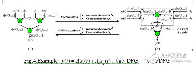
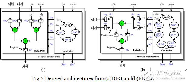
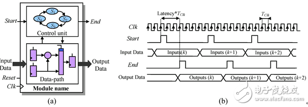
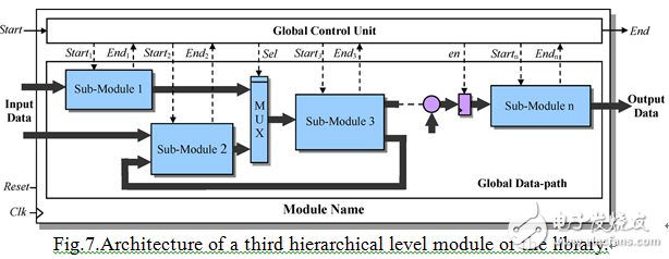
As mentioned earlier, the simulation steps have been demonstrated in the Matlab-simulink software environment. Its objectives are: to change the functionality of the complete control system; to find the appropriate sampling period and fixed-point format improvements for each control variable, as required by the control system's defects. With the use of simulated continuous time modules, the development of functional modules can cause these functions to change successfully. However, the parameterization of each combined digital algorithm is obtained under the influence of the study of the sampling period and the fixed-point format. With this in mind, the choice of each fixed-point format is derived from an adaptable method [30], [31]. At this level, simulation is implemented in the development of a digital fixed-point model using the system-generated toolbox [32]. However, for each proposed second level module, the concept of data flow graph (DFG) is proposed. DFG is a graphical representation of an algorithm that includes an untimed specification consisting of points and edges. Each point represents a simple algorithmic operation, or a simple mathematical or logical function, with each edge corresponding to a data conversion. For example, as shown in Figure 4(a), the DFG graph of the second algorithm level shows the following functions: (1) As shown in the association graph DFG, two applications can be completed in the parallel mode, but the additional applications depend on The results of both applications have been achieved and can only be achieved if the results of both applications are achieved. Therefore, the DFG graph clearly represents the data parallelism and the potential parallelism of the algorithm. Figure 3 shows the different steps presented. It is worth noting that, so far, the choice of target devices has not been available, because module separation and fixed-point improvement are also applicable to DSP controllers [33]. The step optimization is based on the A3 technology [28]. The purpose of this method is to achieve the hardware structure optimization of the given algorithm under the space and time constraints if the FPGA-based design is performed. In each DFG diagram, some operations are used several times. If some operations use n times, then A3 will perform factorization but still apply to this operation, except that it only uses m times, and m For each module in the library, you need to define a data channel and a control device. The data channel in the structure can be used to replace the data bus between the operator corresponding to the node in the final graph and the operator corresponding to the edge. The data bus conversion is controlled by the control device, which may simply be referred to as a finite state machine (FSM). The structures of Figures 5(a) and 5(b) correspond to DFG and FDFG in Figure 4, respectively. It is worth noting that the data channel that has been obtained is actually a pseudo-copy of the corresponding graphic. In addition, the structure of the factorization is much larger than the structure of the structure that cannot be decomposed. The first step in verification is to use the Modelsim and Maltab software tools together for process operation simulation. This step allows the benign functions in the design structure to be modified by writing VHDL, and can be tested through a series of experimental platform input waveforms. The second verification step is performed at the system level by hardware in the loop operation step. The purpose of this process is to ensure the first experimental guarantee, which is completed in real time by hardware in the test structure, as shown in FIG. It mainly consists of three modules. The first is to generate the promotion mode and save it in the FPGA memory module. These facilitation models are directly derived from the simulation phase and can be further compared to the simulation system. The second module is the structure that is used for testing, and the third module is a communication interface module that connects the FPGA to the PC host. The computational output of this structure should be tested centrally and sent to the host PC via the communication interface for comparison with the results of the simulation in the Matlab environment. Once this test result is verified successfully, the structure of the secondary design will be applied to the actual. 1.4GB ( 1x 4GB Module ) | DDR3 1600 MHz PC3-12800 / 12800S | DDR3 SO-DIMM ( 204-Pin ) | Non-ECC Unbuffered ddr3 4gb,ddr3 4gb ram,ddr3 4gb ram price,4gb ddr3,ddr3 4gb 1600mhz Easy Electronic Technology Co.,Ltd , https://www.pcelectronicgroup.com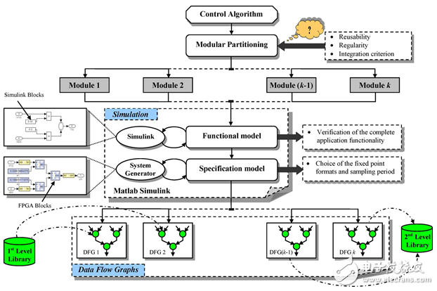
2.High performance Memory RAM upgrade designed for Laptop, Notebook, & All-in-One Computers
3.Easy to install and compatible for select (not limited to) Acer, Alienware, Apple, ASRock, ASUS, Dell, DFI, Fujitsu, Gateway, Gigabyte, HP, HP Compaq, Intel, Lenovo, LG, MSI, Panasonic, QNAP, Samsung, Sony, Supermicro, Synology & Toshiba Models
4.All modules undergo quality assurance testing to ensure dependable and reliable performance | Please verify the supported memory (RAM) specifications of your system prior to purchase to ensure compatibility
5.A-Tech provides a Lifetime Warranty for all orders & offers complimentary United States based Tech Support before, during, & after your purchase
FPGA-based AC motor driver current controller 3
Simulation and algorithm improvement steps