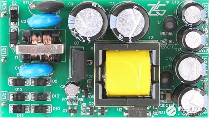
For the development of switching power supplies, PCB design plays an important role. A poor PCB, poor EMC performance, large output noise, weak anti-interference ability, and even basic functions are flawed. A little different from other hardware circuit PCBs, the switching power supply PCB has its own characteristics. This article will combine engineering experience to briefly talk about some of the most basic principles of switching power supply PCB layout. 1, spacing Line spacing must be considered for high voltage products. The spacing that meets the required safety requirements is of course best, but in many cases the spacing is determined by experience for products that do not require certification or that do not meet the certification requirements. What is the appropriate spacing? It is necessary to consider whether the production can guarantee the cleanness of the board surface, the humidity of the environment, and other pollution. For the mains input, even if the board surface is clean and sealed, the MOS tube drain source is close to 600V, and less than 1mm is actually dangerous! 2, the edge of the board components Chip capacitors or other fragile devices on the edge of the PCB must be placed in consideration of the direction of the PCB board. The stress ratio of the device is shown in the various placement methods. Figure 1 Stress comparison of the device when it is split It can be seen that the device should be far away and parallel to the edge of the board, otherwise the components may be damaged due to the PCB board. 3, the loop area Whether it is input or output, power loop or signal loop, it should be as small as possible. The power loop emits an electromagnetic field that will result in poor EMI characteristics or large output noise. At the same time, if it is received by the control loop, it is likely to cause an abnormality. On the other hand, if the power loop area is large, the equivalent parasitic inductance will increase, which may increase the drain noise spike. 4, the key trace Due to the di/dt effect, the inductance at the dynamic node must be reduced, otherwise a strong electromagnetic field will be generated. To reduce the inductance, the main reason is to reduce the length of the wiring, and increase the width is less effective. 5, signal line For the entire control section, route it away from the power section. If the two are close by other restrictions, the control line should not be parallel with the power line. Otherwise, the power supply may work abnormally and oscillate. In addition, if the control line is very long, the pair of wires should be brought close to each other, or they should be placed on both sides of the PCB and directly opposite each other, thereby reducing the loop area and avoiding interference by the electromagnetic field of the power portion. Figure 2 illustrates the correct and erroneous signal line routing method between the two points A and B. Figure 2 shows the correct and wrong signal line routing method. Of course, the vias for connection should be minimized on the signal line! 6, copper plating Sometimes copper is completely unnecessary and should be avoided. If the copper area is large enough and its voltage is constantly changing, on the one hand it may act as an antenna to radiate electromagnetic waves to the surroundings; on the other hand, it is easy to pick up noise. Usually only copper is allowed on the static node, for example, copper is plated on the output "ground" node, which can increase the output capacitance equivalently and filter out some noise signals. 7, mapping For a loop, copper can be plated on one side of the PCB, which automatically maps to the other side of the PCB, minimizing the impedance of this loop. This is like a set of impedances with different impedance values ​​connected in parallel, and the current will automatically select the path with the least impedance flow. In fact, it is possible to connect wires on one side of the control part of the circuit, and copper on the other side of the "ground" node, and the two faces are connected by via holes. 8, output rectifier diode If the output rectifier diode is close to the output, it should not be placed parallel to the output. Otherwise, the electromagnetic field generated at the diode will penetrate the loop formed by the power supply output and the external load, increasing the measured output noise. Figure 3 Correct and wrong diode placement direction 9, ground wire The wiring of the ground wire must be very careful, otherwise it may cause deterioration of EMS, EMI performance and other performance. For the "ground" of the switching power supply PCB, at least the following two points: (1) power ground and signal ground, should be connected at a single point; (2) there should be no ground loop. 10, Y capacitor The input and output often connect to the Y capacitor. Sometimes, for some reason, it may not be possible to hang it on the input capacitor ground. Remember to connect it to a static node, such as the high voltage side. 11, other In actual power supply PCB design, other problems may be considered, such as "the varistor should be close to the protected circuit", "common mode electric induction increases the discharge tooth", "chip VCC power supply should increase the ceramic capacitor", etc. . In addition, whether special treatment, such as copper foil, shielding, etc., is also needed in the PCB design stage. Sometimes there are often situations in which multiple principles conflict with each other. Satisfying one of them will not satisfy others. This requires engineers to apply existing experience and determine the most appropriate wiring according to actual project requirements! Maskking(Shenzhen) Technology CO., LTD , https://www.szelectroniccigarette.com