1.Shape:Conical ,Multi-pyramidal,Columniform,polygonal or conical
2.Material:steel plate.stainless steel compound plate,stainless steel plate,ect.(anticorrosion treatment with hot galvanization,also color polyester power could be coated on the surface)
High strength low alloy steel Q235,Q345,GR65,GR50 to ensure the mechanical properity of microelement in order to ensure the quality of galvanization (other materials are also avaliable on request)
3.Jointing of pole with insert mode,innerflange mode,face to face joint mode
4.Design of pole :against earthquake of 8 grade ,aganist wind pressure of 160
5.Minimum yield strength:355 mpa
6.Minimum ultimate tensile strength :490 mpa
7.Max ultimate tensilestrength:620 mpa
8.Certificate:ISO9001-2000
9.Length:Within 14m once forming without slip joint
10.Welding:It has past flaw testing.Internal and external double welding makes the welding beautiful in shape
11:Packages:Our poles as normal cover by Mat or straw bale at the top and bottom ,anyway also can following by client required , each 40HC or OT can loading how many pcs will calculation base on the client actually specification and data
Our lighting equipment are made from quality sheet from bending,forming,automatic welding and hot galvanization.We can reach one-run machining length of 14m,and can bend sheet thickness up to 25mm.We adopt advanced welding procedures ,automatically weld main joints and reach rank-II welding quality.
Galvanized Steel Pole,Galvanized Steel Electric Pole,Monopole Galvanized Steel Electric Pole,Galvanized Steel Street Lighting Poles YIXING FUTAO METAL STRUCTURAL UNIT CO.,LTD( YIXING HONGSHENGYUAN ELECTRIC POWER FACILITIES CO.,LTD.) , https://www.chinasteelpole.com
Some applications require a stable output voltage, which may be higher or lower than the input voltage range. This is common in battery-powered systems where the input voltage changes over time.
Conventional methods include increasing the battery voltage and then lowering it to the desired value. This can obtain a stable voltage from the battery, regardless of the original level of the battery.
However, such methods have some drawbacks: increasing the number and space of components, increasing costs, reducing reliability, and reducing the efficiency of power transfer. In this article, we will introduce you to a better way to obtain a stable voltage from various voltage input sources.
One type of converter that can perform the required function is the non-insulated SEPIC, which is an acronym for Single-Ended Primary Inductance Converter. This converter can reduce or increase the input voltage.
This article outlines the operation of a SEPIC circuit controlled by a regulator based on the National Semiconductor LM2623 ratio adaptive gated oscillator.
SEPIC circuit: Principle of operation All inductor and capacitor waveforms in a switching DC / DC converter are composed of a DC component and a small amount of undesired AC components, which are caused by incomplete attenuation of switching harmonics:
Where X (t) can be the current or voltage of an inductor or capacitor. However, the output switching ripple, as well as the inductor and capacitor ripple waveforms, should be sufficiently small in any well-designed converter, because generating a DC output is its main purpose. Therefore, in principle, the assumption that the magnitude of the switching ripple is much smaller than the DC component is correct. ![]()
The output of the general waveform provided in this converter approximates the following representation: ![]()
This is the so-called small ripple approximation. ![]()
Definition relationship between inductor and capacitor: 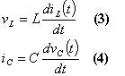
Let's integrate during the switching cycle:
At steady state, the net change in inductor current and capacitor voltage within one switching cycle must be zero, so [Equation 5] and [Equation 6] become: 
The equivalent form is obtained by dividing both ends of [Equation 7] and [Equation 8] by the switching period: 
This shows that in equilibrium, the average inductor voltage and capacitor current must have a zero DC component. 
This can be explained intuitively. If a DC voltage is applied to the inductor, the flow rate will continue to increase, and the inductor current will increase indefinitely. Similarly, if direct current is applied to the inductor, the capacitor will continue to charge and its voltage will increase indefinitely.
Equations [Equation 9] and [Equation 10] are called the inductor volt-second balance and capacitor charge balance principles.
The principles introduced so far, Ban is now used to derive the steady-state DC component of the inductor current and capacitor voltage of the SEPIC circuit. Also find the magnitude of voltage and current ripple. We will assume that all components are ideal; parasitic components, for example, the source of power loss is ignored.
The actual situation of a SEPIC circuit using a switch and a diode is illustrated graphically in Figure 1. 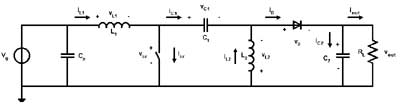
Figure 1: SEPIC circuit.
This converter utilizes four dynamic energy storage elements: L1, L2, C1, and Cout.
The behavior of the SEPIC circuit strongly depends on the continuity of the current in the inductor and the voltage in the capacitor. Because there are many different modes of operation, it determines whether the inductor current and capacitor voltage are continuous or discontinuous. Although all modes may exist, the common mode of operation is that the voltage on C1 is continuous, while L1 and L2 are continuous conduction, or intermittent conduction. In this article, we will mention the case where the current in the inductor is never zero: This mode of operation is called continuous conduction mode (CCM). CCM produces a smaller current ripple, which implies that there are lower stresses on the passive components of the circuit, and there is lower electromagnetic interference.
As described in Figure 2a, when the switch is closed, energy is transferred from the input source to L1 and from C1. During this time, C2 provides the necessary energy to the load. When the switch is finally opened, as shown in Figure 2b, the energy stored in L1 and L2 is released to C1, C2, and the load through the diode. 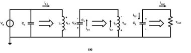
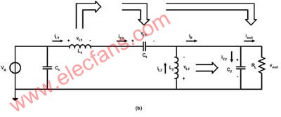
Figure 2: Power flow when the switch is closed (a) and open (b)
When the switch is closed (Figure 2a), the inductor voltage and capacitor current with randomly defined polarities are as follows: 
According to the small ripple approximation, we assume that the switching ripple values ​​of vg, vc1, iL2 and vouy are smaller than the corresponding DC components Vg, Vc1, IL2 and Vout. 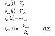
When the switch is turned on (Figure 2b), the inductor voltage and capacitor current become: 
The approximate output of [Equation 13] is: 
The inductor voltage and capacitor current waveforms based on [Equation 12] and [Equation 14] are illustrated graphically in FIG. 3. 
Figure 3: SEPIC circuit waveform.
We now set the DC component or average value of the waveform in Figure 3 to zero in order to find steady-state conditions in the converter: 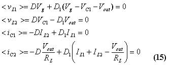
Among them, represents the working cycle of the switch, is the complement of the working cycle, and is defined as. The solution to this equation system can be expressed as follows: 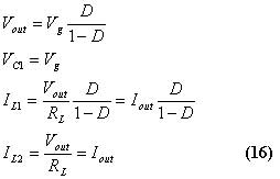
In order to complete our steady-state analysis, we will estimate the magnitude of the switching ripple of the inductor current and capacitor voltage. These are described in Figure 4. 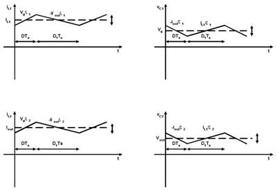
Figure 4: SEPIC ripple waveform.
The range of the waveform can be derived by analysis in the first sub-interval: 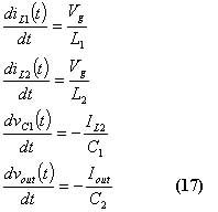
Since we know that the length of the first interval and the waveform in the steady state are symmetrical with their average value, we can calculate the ripple value: 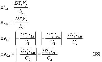
These expressions can be used to select the values ​​of L1, L2, C1, and C2 in order to obtain the desired value of the switching ripple value.
Ratio adaptive gating oscillator voltage regulator
National Semiconductor ’s LM2623 is a switching regulator that includes low-side NMOS switches and is designed for DC / DC converters, such as boost converters and SEPIC.
As described in Figure 5, the control mode of the regulator consists of a hysteresis comparator with oscillator enabled, which can drive the switch. 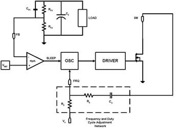
Figure 5: LM2623 block diagram.
You can refer to Figure 6 to understand the basic operation of the device. 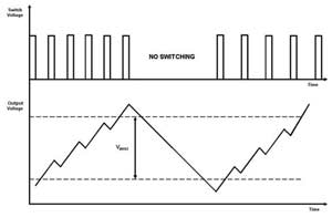
Figure 6: Ideal voltage regulator waveform.
The duty cycle depends on the external passive network composed of R5 and C3. If R5 and C3 remain disconnected, the default duty cycle is approximately 17%. This is achieved by setting the duty cycle to exceed the maximum value required by the application. The system switching continues until the output voltage reaches the upper limit. When the output reaches the lower limit, the system switching restarts. This type of operation mode adopts the so-called pulse frequency modulation technique. When current flows through the inductor per switching cycle, the inductor stores more energy per switching cycle. When the upper voltage limit is reached, the output voltage usually exceeds the required voltage because the energy stored in the inductor is being transferred to the output. When the system starts switching again, the output voltage will also undershoot because the energy in the inductor needs to be restored. Large output capacitors and small inductors will reduce ripple in these situations. As a result, the switching frequency generated in the system is not the oscillator frequency, but a lower frequency determined by the load and input / output voltage. This mode of operation is very useful in applications where the load varies greatly.
The output voltage passes through resistors RF1 and PF2 and then sets the output voltage accordingly. Capacitor CF1 directly injects ripple from the output into the comparator. In this way, once the voltage limit is reached, the comparator is triggered, thereby minimizing output overload and underload.
If the load does not change in various ranges, the ratio adaptive function of the LM2623 can be used to implement the so-called cycle-to-cycle PFM operation mode. This technique is used to match the duty cycle of the converter to the duty cycle required for the input to output voltage ratio. The duty cycle is dynamically adjusted to account for changes in the output-to-input ratio. In this way, most of the energy stored in the inductor is transferred to the load during each switching cycle. Modulation is achieved by adjusting the on and off time within each switching cycle to meet the current requirements of the load. The current in the inductor never goes to zero, as in the case of various load changes in a hysteretic operating mode circuit, or during a duty cycle, the input to output voltage ratio does not match. As a result, the output ripple is much lower compared to the hysteresis operation mode. Figure 7 shows a simplified block diagram of the ratio adaptive control mode. For simplicity, we assume that switches are included in the converter block. 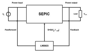
Figure 7: Block diagram of the ratio adaptive control mode.
The duty cycle modulation mechanism can be understood by analyzing the oscillator architecture shown in Figure 8. 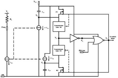
Figure 8: LM2623 oscillator circuit.
Let us assume that the device is enabled, and node A starts very high, which means that the switch is on. In this state, nodes D and E are in high and low states, respectively, Coff discharges through N2, P1 and P2 are off, N1 is on, and node D is connected to node B. VB = VD decreases linearly. At the time constant given by Iosc and the size of Con, nodes A, D, and E become low, low, and high before the NOT gate switches. In this new state, the switch is off, discharging through P1, N1 and N2 are off, and P2 is on, and node D is connected to node C. Vc = VD increases linearly. Under the time constant determined by Iosc and the size of Coff, node A becomes high again before the NOT gate switches.
The switching frequency is determined by Iosc, which is the current mirrored from the constant current source, and its current is set by Vg and R3 and the size of the two capacitors; The ratio sets the duty cycle to 17%.
The ideal state of duty cycle modulation is to modulate the DC current flowing into the frequency pin to slow down the oscillator during the on time and accelerate the oscillator during the off time. The series connected before the switch and the frequency pin behave like a DC source: when the switch is on, it discharges charge from the frequency pin, and when the switch is off, it injects other charges into the same pin. The time constant of charge transfer in two directions is as follows: ![]()
As the input voltage of the converter drops, the AC charge transfer becomes a larger percentage of the oscillator current; the result is an increased duty cycle. By choosing a corresponding value for Ï„, the amount of charge transfer increases because the oscillator slows down due to the falling input.
The following briefly describes empirical methods for selecting external components for frequency and duty cycle modulation.
VgR3 provides the DC drive current for the oscillator: when the resistance value is low, the frequency increases, and when the input voltage value is low, the frequency decreases. Vg at the lowest value R5 is set to zero, and C3 increases until modulation is obtained. C3 determines the maximum charge transfer amount; a smaller R3 value requires a larger value (greater than AC charge transfer) in order to achieve the same duty cycle modulation percentage. Then R5 increases until the duty cycle matches the input-to-output ratio. At this time, Vg increases to its maximum value. If the duty cycle does not decrease enough, R5 will increase until the duty cycle matches the input to output ratio. The input drops again to its minimum value, and if the duty cycle is not high enough, C3 drops. This process will be repeated until the time constant Ï„ allows the duty cycle to change accordingly over the entire input voltage range.
LM2623 SEPIC design example
In this section, we introduce the SEPIC design example of period-to-period PFM modulation mode, with the following specifications: 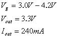
The nominal maximum and minimum duty cycles are as follows: 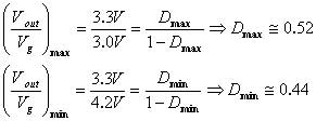
The component of the external passive network is equal to: 
These components set the switching frequency between 1.6MHz and 1.8MHz and allow the duty cycle to vary between the minimum and maximum desired values.
The size of the inductors in SEPIC is usually selected to limit the peak-to-peak ripple current flowing into them and maintain a continuous conduction mode. It is better to choose the latter because it leads to lower electromagnetic interference. The maximum current ripple is usually set between 30% and 50% of the average current flowing through each inductor. As a starting point, we choose a value of 40% to estimate the value of inductance: 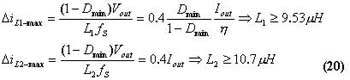
Where η is the correct factor and power loss will be considered due to parasitic effects.
We choose L1 = L2 = 15UH, which can handle the following maximum peak currents: 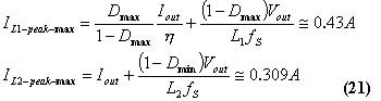
The maximum voltage and current stresses of the switch in this application are as follows:
L 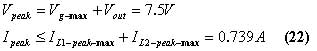
The switches in M2623 have a minimum current limit of 2.2A and a maximum voltage capability of 14V, respectively.
When the switch is closed, the output diode turns on and provides a path for the inductor current. Important criteria for selecting rectifier diodes include: rapid switching, breakdown voltage, rated current, and low forward voltage drop to minimize power consumption. The best solution is a Schottky diode. The breakdown voltage must be greater than the maximum input voltage and output voltage, and some tolerance should be added for normal and spikes. The rated current should be at least equal to the sum of the maximum peak currents in the two inductors: Generally, the rated current will be higher because power consumption and junction temperature limitations govern the choice of device. For our example, we chose a Schottky diode with a rated current of 3A and a breakdown voltage of 40V.
The function of capacitors is to store energy in their electric field; therefore, from a quality perspective, the function of capacitors is to try to maintain a constant voltage. The SEPIC capacitor C1 provides energy to the inductor L2 during the switching time. Assuming a maximum voltage drop of 5%, the calculated value of C1 is equal to: ![]()
The capacitor selected must be able to handle the rms ripple current: 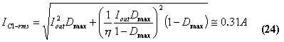
Finally, we select tantalum capacitors 100UF and 22UF ceramic capacitors for C2 and Cin, respectively.
The rms current energy of the two capacitors must be equal to: 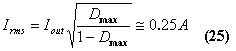
Sometimes it is useful to place the output capacitors in parallel. Ceramic capacitors can bypass high frequency harmonics.
The entire circuit is shown in Figure 9; Figures 10-13 show the experimental current waveforms of the two inductors at different input voltages. 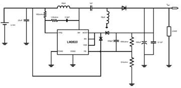
Figure 9: SEPIC circuit of LM2623. 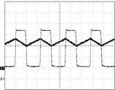
Figure 10: Current waveform of L1 switching signal when Vg = 3.0V. 1) VSW, 2V / div, DC; 2) Inductor current, 100mA / div, DC; T = ns / div 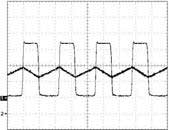
Figure 11: Current waveform of L2 switching signal when Vg = 3.0V. 1) VSW, 2V / div, DC; 2) Inductor current, 100mA / div, DC; T = ns / div 
Figure 12: Current waveform of L1 switching signal when Vg = 4.2V. 1) VSW, 2V / div, DC; 2) Inductor current, 100mA / div, DC; T = ns / div 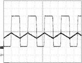
Figure 13: Current waveform of L2 switching signal when Vg = 4.2V. 1) VSW, 2V / div, DC; 2) Inductor current, 100mA / div, DC; T = ns / div
in conclusion
Although the SEPIC topology places higher stresses on switches and diodes than other topologies, there is no need to use transformers for voltage conversion, but through lower-cost inductors. This type of converter is also very useful in boost applications that require real shutdown, because the input and output voltages are DC isolated by coupling capacitors.
Provided the SEPIC design example of National Semiconductor's LM2623 regulator. If the load does not change within a certain range, you can use external components to repair the switching frequency and allow the duty cycle to vary with input changes. In this way, the behavior of the converter is similar to a typical PWM modulation converter. The difference of this converter is that no compensation is required because the PFM architecture is very stable.

SEPIC controlled by LM2623 ratio adaptive gated oscillator
Introduction