OEM needs smaller and more diverse packaging options to meet product design challenges and maintain cost competitiveness in their respective markets. Ball grid array (BGA) packaging is becoming more and more popular to meet these design requirements. In addition, they are ideal solutions, because I/O connections are located inside the device, increasing the ratio of pins to PCB area. In addition, BGA with strong solder balls is stronger than QFP lead, so it is more robust.
With today's electronics technology, the demand for I/O availability poses a number of challenges, even for experienced PCB designers, due to multiple exit routes.
Additional Information BGA PCB Bare PCB,BGA PCB,BGA Circuit Board,BGA PCB Design JingHongYi PCB (HK) Co., Limited , https://www.pcbjhy.com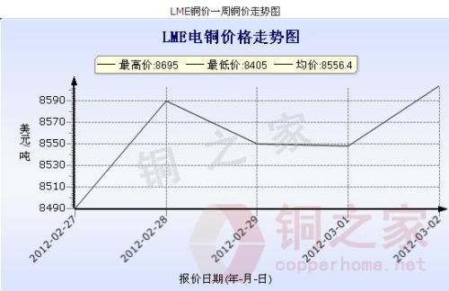 Date Name Lowest Price High Price Daily Average Price Change
2012-2-27 LME copper 8420 8560 8490 53
2012-2-28 LME copper 8490 8689 8589.5 99.5
2012-2-29 LME copper 8405 8695 8550 -39.5
2012-3-1 LME Copper 8448 8648 8548 -2
2012-3-2 LME copper 8537 8670 8603.5 55.5
Ball Grid Array (BGA), a type of surface-mount packaging (a chip carrier) used for integrated circuits.
Ball-Grid Array (BGA) Packages Become PCB Design Mainstream
BGA PCB Design Guidelines And Rules
BGA PCB Design Rules
In order to keep up with the technological progress of chip manufacturers, BGA software packages for embedded design have made remarkable progress in the past few years.
This special type of packaging can be decomposed into standard BGA and micro BGA.
Correct BGA partitioning first takes into account uniformity of the partitioning, itself. Because, precise BGA partitioning on a PCB is a crucial design aspect to minimize or eliminate crosstalk and noise, as well as manufacturing issues.
Memory signals need special consideration during BGA partitioning. They need to be away from oscillating signals and power supply switching. This is important because memory signals needs to be clean. If traces carrying these signals are in the proximity of oscillating signals or switching power supply signals, they produce ripples in the memory signal traces, thereby reducing system speed. The system is operational, but at less than optimal speed levels.
BGA PCB Design Guidelines
BGA Design Strategy 1: Define an appropriate exit path
The main challenge for PCB designers is to develop appropriate exit routes without causing manufacturing failures or other problems. Several PCBs need to ensure proper fan-out wiring strategies, including pad and pass size, I/O pin number, layers required for fan-out BGA and line width spacing.
BGA Design Strategy 2: Identify the Layers Required
Another question is how many layers the PCB layout should have, which is by no means a simple decision. More layers mean higher overall cost of the product. On the other hand, sometimes you need more layers to suppress the amount of noise PCB may encounter.
Once the alignment and space width of PCB design, the size of through holes and the alignment in a single channel are determined, they can determine the number of layers they need. Best practice is to minimize the use of I/O pins to reduce the number of layers. Usually, the first two outer sides of the device do not need through holes, while the inner part needs to arrange through holes below them.
Many designers call it dog bones. It is a short path of the BGA device pad, with a through-hole at the other end. The dog bone fan comes out and divides the equipment into four parts. This allows the remaining internal padding to be accessed by another layer and provides escape paths away from the edge of the device. This process will continue until all mats are fully developed.

BGA Package Types
There are six different BGA packages.
1. Moulded Array Process Ball Grid Array (MAPBGA): It is a BGA package which provides low inductance and simple surface mounting.
2. Plastic Ball Grid Array (PBGA): Again, this BGA package provides low inductance, simple surface mounting, high reliability and is cheap.
3. Thermally Enhanced Plastic Ball Grid Array (TEPBGA): Just like its name sound, this BGA package can handle great levels of heat dissipation. Its substrate has solid copper planes.
4. Tape Ball Grid Array (TBGA): You can use this BGA package as a solution for medium- to high- end applications.
5. Package on Package (PoP): It will permit you to put a memory device on some base device.
6. Micro BGA: This BGA package is quite small when compared with standard BGA packages. Currently, you will see 0.65, 0.75 and 0.8 mm pitch size dominating in the industry.
BGA PCB Assembly
Previously, Engineers were not sure whether PCB BGA assembly would be able to achieve the reliability level of traditional SMT methods. However, at present, this is no longer a problem, because BGA has been widely used in Prototype PCB assembly and mass production PCB assembly.
You will need to use reflow methods to solder a BGA package. Because only reflux method can ensure solder melting under BGA module.
We have a wealth of experience handling all types of BGAs, including DSBGA and other Complex Components, from micro BGAs (2mmX3mm) to large size BGAs (45 mm); from ceramic BGAs to plastic BGAs. We are capable of placing minimum 0.4 mm pitch BGAs on your PCB.
PCB BGA Advantages
With PCB BGA, you will get the following advantages:
1. BGA package eliminates the issue of developing small packages for ICs with lots of pins.
2. Again, when compared with packages with legs, The BGA package has a lower thermal resistance when placed on the PCB.
3. Do you know which property causes unwanted signals distortion in high-speed electronic circuits? The unwanted inductance in an electrical conductor is responsible for this phenomenon. However, BGAs have very little distance between PCB and the package which in turn leads to lower lead inductance. Thus, you will get top-class electrical performance with pinned devices.
4. With BGAs, you can effectively utilize your Printed Circuit Board space.
5. Another advantage that will come with BGA is the reduced thickness of the package.
6. Last but not least, you will get enhanced re-workability because of bigger pad sizes.

Via in PAD(VIP) PCB
6 Layer BGA PCB