![]()
MOSFET imported original FET
![]()
Supply 0603 blue LED

The following is a circuit diagram of [Field Effect Tube Naming, Parameters, Types, and Pin Diagrams].
First, the model name naming method of the field effect transistor. The second naming method is CS××#, where CS stands for FET, XX represents the serial number of the model, and # indicates different specifications within the same model. For example, CS14A, CS45G, etc.
Second, the parameters of the FET:
- I DSS – Saturated drain current. This refers to the drain-source current when the gate voltage UGS = 0 in a junction or depletion insulated gate FET.
- UP – Pinch-off voltage. It’s the gate voltage at which the drain-source channel just turns off in a junction or depletion-type insulated gate FET.
- UT – Threshold voltage. This is the gate voltage needed to turn on an enhancement-type insulated gate FET.
- gM – Transconductance. It measures how much the drain current changes in response to a change in the gate-source voltage. gM is crucial for evaluating the amplification capability of the FET.
- BUDS – Drain-source breakdown voltage. This is the maximum voltage the FET can withstand between drain and source with the gate-source voltage held constant.
- PDSM – Maximum power dissipation. This is the highest power that can be dissipated without degrading performance. Operating conditions must stay below this value.
- IDSM – Maximum drain current. This is the highest allowable current between drain and source during normal operation.
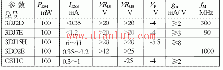
Common parameters for several typical FETs are shown in the image below.
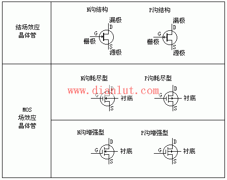
Third, classification of FETs: Based on semiconductor materials, FETs are divided into junction type and insulated gate type, and further categorized by channel type (N-channel or P-channel). They can also be classified as depletion mode or enhancement mode. Junction FETs are typically depletion type, while insulated gate FETs (like MOSFETs) can be both. The image below shows the classification of FETs.
Fourth, the role of FETs:
- FETs have high input impedance, making them ideal for impedance matching in amplifier circuits.
- They can function as variable resistors.
- They can act as constant current sources.
- They can be used as electronic switches.
Fifth, testing FETs:
- Pin identification for JFETs: Use a multimeter in R×1k mode. When two pins show equal resistance, they are the drain and source; the remaining one is the gate. For 4-pin JFETs, the fourth pin is the shield (grounded).
- Determining the gate: Touch one electrode with the black lead and the others with the red lead. If both readings are low, it's an N-channel FET, and the black lead is the gate.
- Estimating gain: Set the meter to R×100, connect red to source and black to drain. Pinch the gate with your finger to apply body-induced voltage. A large needle swing indicates good gain. If no movement, the FET may be damaged.
- MOSFET test precautions: Always use an insulated tool to avoid damaging the gate due to static charge. After testing, short the gate and source to discharge any stored charge.
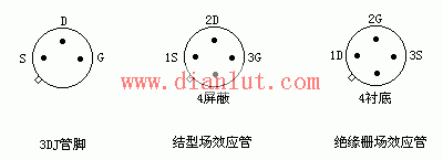
The pin configuration for common JFETs and MOSFETs is shown in the image below.
(Editor: Circuit Diagram)
Dell Certified Refurbished,Refurbished Dell Computers,Used Dell Computers,Used Dell Laptops For Sale