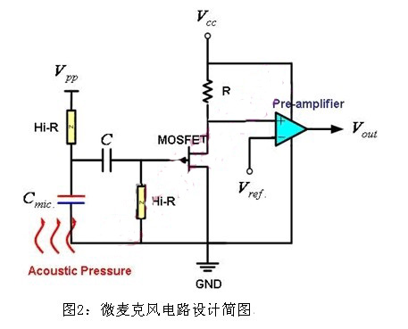
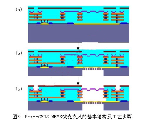
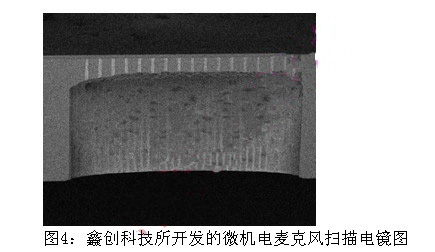
With the rise of smart phones, the demand for sound quality, lightness and shortness has been receiving more and more attention. In recent years, noise suppression and echo cancellation technologies have been widely used to improve the quality of sound. Capacitive MEMS microphones are fabricated from silicon semiconductor materials compared to conventional electret microphones (ECMs), which facilitate the integration of analog amplifier circuits and ADC (∑-Δ ADC) circuits to implement analog or digital MEMS microphone components, as well as manufacturing Miniaturized components are ideal for use in thin, light and portable devices. This article will introduce the design and manufacture of CMOS MEMS microphones, and compare the differences between pure MEMS and CMOS micro-introduction microphones. Capacitive micro-microphone principle The MEMS micro-microphone is a miniature sensor. The principle is to use the pressure gradient generated by the sound change to cause the acoustic diaphragm of the capacitive micro-microphone to be deformed by the sound pressure, thereby changing the capacitance between the acoustic diaphragm and the silicon back plate. The change of the capacitance value is converted into a voltage value output change by the capacitor voltage conversion circuit, and then the MEMS sensor generates a voltage amplification output through the amplification circuit, thereby converting the sound pressure signal into a voltage signal. Here, a high-impedance resistor must be used to provide a bias voltage VPP for the MEMS sensor to generate a fixed charge on the MEMS sensor. The final output voltage will be proportional to the VPP and diaphragm deformation Δd. The deformation of the diaphragm is related to its rigidity. The lower the rigidity, the larger the deformation. On the other hand, the output voltage is inversely proportional to d (air gap). Therefore, the lower the air gap, the better the output voltage and sensitivity, but this will be affected. Limited to the pull-in voltage of the MEMS sensor, which is limited by the maximum limit of the MEMS sensor's electrostatic field (Figure 1). CMOS MEMS microphone circuit design In CMOS micro-microphone design, the circuit is a very important part that will affect the operation, sensing, and sensitivity of the micro-microphone. Taking Figure 2 as an example, the induced charge of the electret condenser micro-microphone is generated by the electret charge provided by the electret material itself, while the condensed condenser micro-microphone extracts a bias voltage from the operating voltage of the CMOS. The acoustic diaphragm is then supplied to the micro-microphone through a high-impedance resistor to provide a fixed source of charge. At this time, if the acoustic diaphragm is driven by the sound pressure to cause a displacement change, the voltage of the electrode plate (sensing end) will change. Finally, by amplifying the signal through the circuit amplifier, the circuit design of the analog microphone can be realized; if a ∑-Δ ADC analog-to-digital conversion circuit is added, the circuit design of the digital microphone can be completed (the output signal of the general digital microphone is 1 bit). PDM output). CMOS MEMS Microphone Process Classification From the perspective of the manufacture of MEMS microphones, MEMS components integrated with CMOS circuits can be classified into three types at the current technical level. Pre-CMOS MEMS process: first make MEMS structure, then make CMOS components; Intra-CMOS MEMS process: CMOS and MEMS component process hybrid manufacturing; Post-CMOS MEMS process: first realize CMOS components, then MEMS structure manufacturing. In general, the first two methods cannot be performed in a traditional fab, while Post-CMOS MEMS can be produced at a semiconductor foundry. Figure 3 outlines the manufacturing of Post-CMOS MEMS. Special care must be taken in the Post-CMOS MEMS process to prevent additional thermal or high temperature processes from affecting the physical properties of the CMOS components and the stress state of the MEMS so as not to affect the initial stress of the diaphragm. Xinchuang Technology Co., Ltd. has overcome many technical problems and completely uses standard CMOS technology to simultaneously manufacture circuit components and MEMS microphone structures. After the CMOS portion is completed, the back side of the chip is ground to the appropriate thickness to meet the package requirements. Finally, the sacrificial oxide is removed using a hydrofluoric acid solution (HF) to release the suspended structure. In addition, an etching method that completely removes the sacrificial material without damaging the microphone diaphragm should be considered in the design, and sticking between the microphone diaphragm and the back electrode plate should be avoided. Sticky phenomenon: Since the distance between the microphone diaphragm and the back electrode plate is only a few micrometers, at this size, when the surface tension, van der Waals force, electrostatic force, ion bond and the like are greater than the restoring force of the microphone diaphragm, the microphone The diaphragm will be permanently deformed and attached to the back electrode plate, so that vibration cannot be generated. In general, the main causes of the viscous structure of MEMS suspension structures can be divided into two categories: the first type occurs after the microphone diaphragm is released, and the microphone diaphragm is affected by the surface tension, so it is pulled closer to the back electrode plate. If the surface force such as van der Waals force or hydrogen bonding force is greater than the restoring force of the microphone diaphragm at this time, the structure will be sticky and unable to recover; the second type is that the suspension structure is subjected to external force or electrostatic attraction during use. Stickiness can also occur in areas where the surface force is greater than the restoring force. Therefore, in the structural design, special consideration must be given to the structural deformation of the microphone diaphragm after release, and it is strengthened in important structural parts, and special design is used to reduce the occurrence of stickiness. Differences between pure MEMS and CMOS processes The MEMS micro-microphones developed by most companies are mainly divided into two types: the first one is to manufacture MEMS ICs by professional MEMS foundries, and an ASIC amplifier is used to package MEMS ICs and ASIC ICs into MEMS by SIP packaging. Microphone chip. This part must protect the diaphragm from being damaged during the IC packaging process, and its packaging cost is relatively high. The other is to use the CMOS fab to fabricate the ASIC part and then use the post process to form the structural part of the MEMS. Its MEMS process technology does not seem to be able to be completed in standard CMOS fabs, mainly because the diaphragm needs to deposit high molecular polymer materials, and polymer materials have not been used in current standard semiconductor IC processes. In addition, after the CMOS process is completed, the diaphragm is etched on the front side of the chip and the cavity and acoustic holes are etched on the back side. This step is done by Carrier Wafer, which has not yet been created in standard CMOS foundries. At present, the biggest issue is how to break through the packaging technology of these two forms of MEMS microphones. Its patents are controlled by micro-microphone companies in the United States. Therefore, the market share of MEMS microphones is mainly distributed among a small number of companies. Xinchuang Technology adopts the method of forming a cavity and an acoustic hole from the back of the chip as a release of the MEMS structure after the CMOS process is completed. This part eliminates the need for special machines and materials and can be completed in existing CMOS fabs, thus reducing development costs. In addition, Xinchuang Technology's products can directly integrate CMOS circuits and micro-microphones on the same chip using wafer-level packaging technology, which also avoids damage to the diaphragm during the packaging process (Figure 4). MEMS microphones have been replaced by ECM microphones, which are widely used in mobile phones (especially smart phones). The main reason is that MEMS microphones have the advantages of good weather resistance, small size and easy digitization. The MEMS microphone is made of a semiconductor material and has stable characteristics and is not affected by the temperature and humidity of the environment, so that stable sound quality can be maintained. The temperature at which the electronics are assembled in a tin furnace is as high as 260 ° C, which often destroys the diaphragm of the ECM microphone and must be reworked, which adds additional cost. The use of MEMS microphones does not affect the material due to the high temperature of the tin furnace, and is suitable for automatic assembly of SMT. After digitizing the microphone signal, it can perform signal processing such as denoising, sound bundling, and echo cancellation to provide excellent call quality. At present, a number of smart phones have adopted digital technology, and there are also signs of accelerated adoption in feature phones. In addition, notebook computers are currently the mainstream of MEMS microphones, and set-top box manufacturers are also actively trying to apply MEMS microphones to the development of voice-activated set-top boxes.
The LED projector lamp is used to specify the luminance above the surrounding environment, and also called the spotlight.Usually, it can be aimed at any direction and has a structure that is not affected by climatic conditions.It is mainly used for large area operation field, building outline, stadium, overpass, monument, park and flower bed.As a result, almost all outdoor use of large areas of lighting can be seen as a projector lamp.
Description of products
1. Fashionable, modern appearance design, make lamps and lanterns also become a work of art, with the environment perfect union.
2. The main material of the luminaire is made of high strength die-casting aluminum material, and the surface anti-aging electrostatic spraying process, Self-cleaning and anti-corrosive.
3. Tempered glass cover with high strength and impact resistance.
4. The lamp can be configured white or monochromatic RGB, gorgeous lighting effects, color purity, powerful change.
5. The lamp body is made of high - die cast aluminum material, surface electrostatic spraying
6. The unique rotatable fixed bolt can be rotated 360 degrees.
7. The light source adopts 1W single RGB light source, LED combination optical arrangement, and the mixing effect is better.
8. The light can be controlled by DMX512, a powerful function of changes in lighting effects.
9.Lamp series, power can be between 18W-36W, can be used for a variety of applications.
Product show
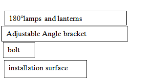
Installation Instruction
Led Tile Slots Lamp,Led Project Lamp,Led Night Lamp,Led Mood Lamp Jiangsu chengxu Electric Group Co., Ltd , http://www.chengxulighting.com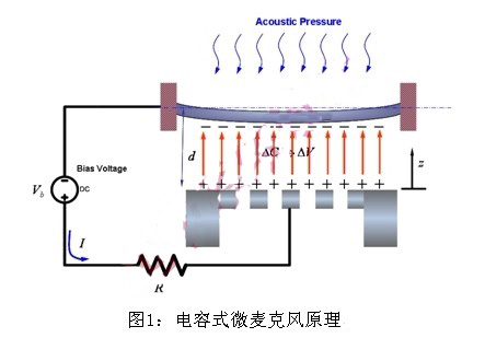


CMOS capacitive microphone design
3 times
Window._bd_share_config = { "common": { "bdSnsKey": {}, "bdText": "", "bdMini": "2", "bdMiniList": false, "bdPic": "", "bdStyle": " 0", "bdSize": "24" }, "share": {}, "image": { "viewList": ["qzone", "tsina", "tqq", "renren", "weixin"], "viewText": "Share to:", "viewSize": "16" }, "selectShare": { "bdContainerClass": null, "bdSelectMiniList": ["qzone", "tsina", "tqq", "renren" , "weixin"] } }; with (document) 0[(getElementsByTagName('head')[0] || body).appendChild(createElement('script')).src = 'http://bdimg.share. Baidu.com/static/api/js/share.js?v=89860593.js?cdnversion=' + ~(-new Date() / 36e5)];