Layout Constraints Today's adjustable speed drive circuits all use frequency converters to adjust the output current to meet the requirements of three-phase motors. The shape and size of the inverter are usually limited by the application. In many cases, the circuit board is very close to the motor, and the height of the motor structure is also limited. In addition, the physical properties of the high-power semiconductor devices used and the shape of the selected package also require sufficient space on the circuit board. The overlapping of the voltage and current generated during the operation of the power semiconductor switch will cause losses and must be eliminated. Although the problem of power dissipation can be improved by adding heat sinks, it also limits the layout of semiconductor devices on the circuit board. Design considerations At present, the development trend of high-power semiconductor devices (such as IGBT and MOSFET) is to continuously reduce the chip size under the premise of improving performance. Reducing the chip size can reduce the parasitic capacitance of the device, thereby increasing the switching rate. Therefore, it is more and more important to deeply study the key loops on the circuit board. Figure 1 is a simplified schematic circuit of two typical switching working modes of a voltage source inverter (VSI). IGBT is the most popular device in high current applications where the switching frequency is limited. The figure above shows the commutation from the high-voltage (HS) freewheeling diode to the low-voltage IGBT. The current is initially in the free-wheeling channel formed by the high-side diode and the corresponding inverting half-bridge IGBT. Figure 1 Simplified commutation circuit Figure 2 Intelligent Power Module Figure 3 Layout recommendations Figure 4 Exaggerated schematic diagram of module installation warpage Component installation considerations In addition to TInyDIP / SMD, the surface of SPM will have some warpage. Figure 4 is an exaggerated illustration of this warpage. The module is fastened to the heat sink with screws that pass through the middle of the surface. If installed properly, this convex surface can ensure that enough heat is transferred from the module to the heat sink. If the tightening screws are applied unevenly, stress may be generated in the module, causing damage to the module or reduced performance. It is recommended to use the screw tightening sequence shown in Figure 4 (pre-tighten in the order of 1 ~ 2 first, and then finally tighten in the order of 2 ~ 1). Generally, the pre-tightening torque is 25% of the maximum rated tightening torque. As long as the heat sink is close to the device, the temperature of the heat sink can be obtained through the built-in thermistor of the SPM, thereby simplifying the design of the circuit board.
We carry various Dvi Controller and computer software to fully customize your led lighting effects using iseeled's DVI LED Controller and Video Wall Controller. These producrts can be used for your night club lighting, bars, theater, movie sets and many more projects require control of a large number of Rgb Led Lights.
Photo show of Dvi Led Controller:
DVI Led Controller Dvi Led Controller,Dvi Controller,Video Wall Controller ,Dvi Led Video Wall Controller Shenzhen Iseeled Technology Co., Ltd. , https://www.iseeledlight.com
The frequency converter is the key technology to meet the energy-saving requirements of EcoDesign. Research by the Electric Power Research Institute (Electric Power Research InsTItute) shows that motors with frequency converters can save up to 40% more energy than motors without frequency converters. Whether it is an induction motor, a permanent magnet synchronous motor, or a brushless DC motor, a sinusoidal current can be generated by the frequency converter. For this reason, the switching frequency must be several orders of magnitude higher than the adjustable output frequency of the inverter. The pulse width modulated output voltage is applied to the inductive load. Therefore, the output current is proportional to the average voltage. The higher the switching frequency, the more beneficial to the inverter; and the smaller the torque fluctuation of the drive, the higher the dynamic response performance and the lower the noise. This requires a fast switching rate, which means that the rate of change of di / dt and dv / dt is usually very high. Therefore, circuit parasitics become a big problem, and designers must work hard to solve this problem in order to meet the current and future EMC standards.
Cost is another constraint that circuit layout must consider. In many cases, double-sided circuit boards are used. Often, only one soldering process can be used for different areas on a circuit board. Therefore, in terms of increasing cost efficiency, surface mount semiconductor devices are an increasingly popular solution. 
Once the low-side gate drive circuit turns on the IGBT, there will be a short-circuit current through the high-side diode and the low-side IGBT. As a result, the diode current decreases and the IGBT current increases accordingly (natural commutation: 1 ~ 2). During switching, the current of the inductive load can be regarded as a constant. Therefore, the stray components are not related to the channel. The switching rate is determined by the conduction of the low-side IGBT and the stray inductance of the half-bridge. To achieve reverse commutation from the low-voltage IGBT to the high-voltage freewheeling diode, the voltage drop on the low-voltage IGBT must be greater than the DC bus voltage to turn on the freewheeling diode. Therefore, the IGBT must be able to withstand high voltage and large current at the same time before commutation with the diode (compulsory commutation: 2 ~ 1).
In Figure 1, the critical current path of the voltage source inverter is marked with red shading, which is characterized by a high di / dt rate of change, which is also reflected in the corresponding gate drive circuit. To ensure the safe operation of the gate drive circuit, it is necessary to minimize stray inductance. Especially for the high-side gate drive circuit, there is a negative pressure caused by the resistive and inductive voltage drop on the low-side diode and the current channel, and the amplitude exceeds the minimum allowable voltage of VS, which will cause abnormal circuit operation.
One solution is to increase the gate resistance to reduce the switching rate, but this will greatly increase the switching loss. In this case, it is necessary to optimize the circuit board layout and make full use of the overall performance of the voltage source inverter. In order to remove the coupling between the power and signal areas, the grounds of the two areas should be separated. The gate driver should be as close to the IGBT as possible without any loops or deviations. The signal path between the microcontroller and the gate drive is not very critical. The discrete IGBT pin leads should be as short as possible to minimize parasitic capacitance and inductance. The arrangement of the six IGBTs and gate drivers packaged together requires careful consideration. In addition, the device on the heat sink needs to be equipped with an appropriate insulating sheet. In many cases, the edge of the circuit board needs a large heat sink.
In order to overcome the above constraints, it is best to use an intelligent power module (IPM), also known as Smart Power Module (SPM®). Figure 2 shows a typical fully enclosed module, which contains a complete three-phase voltage source inverter, and the corresponding gate driver and protection circuit. Using this module saves up to 50% of board space compared to discrete component solutions. In particular, this module requires very few external components, and EMC requirements are considered in the design. The peak and average EMC interference intensity is much lower than traditional design. 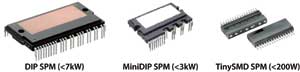
Similar to the discrete component scheme of the voltage source inverter, attention should be paid to the layout of external components when using intelligent power modules. Figure 3 shows some recommendations for MoTIon-SPMTM applications. Due to the fast switching speed of the voltage source inverter, the signal ground and power ground must be separated. The two grounds are connected to each other at a 15V Vcc capacitor. The channel between the Vcc capacitor and the power ground should be narrow to remove coupling. To prevent damage from surges, there should be a low inductance capacitor between pin P and power ground. In addition, because the long lead between the voltage source inverter and the motor will cause high-voltage reflection, some SPM products are equipped with an external gate resistor to adjust the switching rate and minimize reflection. 

")