Fiber Optic Connectors,High-Quality Connectors,Network Solutions Wenzhou Hesheng Electronic Co., Ltd. , https://www.heshengelec.com
The basic principle and debugging principle of jtag
JTAG was originally developed for testing integrated circuits. The core concept involves embedding a Test Access Port (TAP) within the device, which allows access to internal nodes through a dedicated JTAG test tool. This enables multiple devices to be connected in a chain via the JTAG interface, making it possible to test each component individually. Over time, the JTAG interface has also become widely used for In-System Programming (ISP), particularly for devices like flash memory.
JTAG programming is an online process, which means that devices can be programmed directly on the circuit board without the need for prior pre-programming. This simplifies the manufacturing workflow by allowing components to be fixed onto the board and then programmed using the JTAG interface, significantly accelerating the development and testing phases. With this method, all internal components of a PSD chip can be programmed through the JTAG interface.
In simple terms, the working principle of JTAG revolves around defining a TAP inside the device, enabling testing and debugging of internal signals via a specialized JTAG tool.
**Boundary Scan**
Boundary scan technology enhances the JTAG functionality by adding shift register cells at each input and output pin of the chip. These registers are positioned at the chip's boundary, hence the term "boundary scan." During JTAG debugging, these registers isolate the chip from its surrounding circuitry, allowing for observation and control of the input and output signals. For input pins, data can be loaded into the boundary scan register, while for output pins, the signals can be captured by the corresponding register. Under normal operation, these boundary scan registers remain transparent, ensuring that the chip’s regular function is not affected.
Moreover, the boundary scan registers on different pins can be linked together to form a boundary scan chain. This chain allows serial input and output of signals, controlled by clock and control signals, enabling detailed observation and manipulation of the chip's I/O states during debugging.
Around the CPU, the processor includes hardware support for JTAG, providing external access through four key pins: TMS, TCK, TDI, and TDO.
It's important to note that in this context, the term "CPU" refers to the arithmetic processing unit, including only basic components such as internal registers and arithmetic logic units. However, the term "processor" here refers to a CPU expansion chip, not a System-on-Chip (SoC).
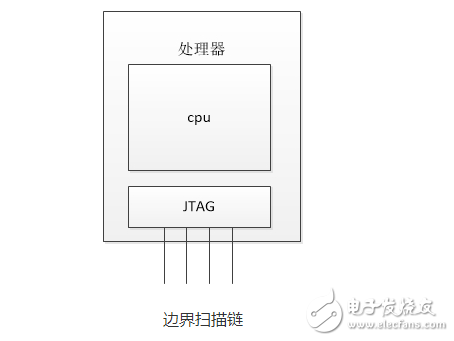
How is JTAG used for chip testing? The most critical element is the boundary scan chain, which is located at the edge of the processor. Since the CPU communicates with peripherals through its pins, all data flows in and out through them. JTAG tests the chip by monitoring the signals on these pins.
The boundary scan chain is embedded at each pin, as shown below:
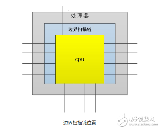
Through the boundary scan chain, when a signal is input, the chain can capture it. When the CPU wants to send a signal, the boundary scan chain can also capture it or allow it to be output directly through the chain.
Whether capturing or outputting signals, an interface is needed to store the data. That’s where TDI and TDO come into play, as shown in the following diagram:
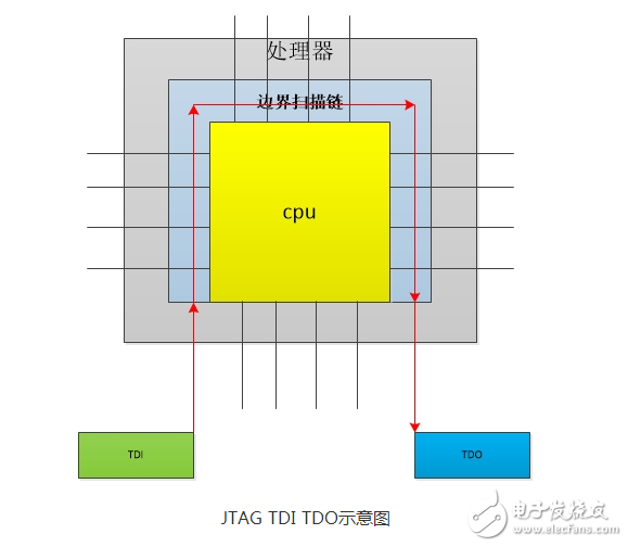
Originally, the boundary scan chain holds the signal on the pin. When we input our own signal through the TDI pin, a shift operation occurs along the path:
**TDI → Boundary Scan Chain → TDO**
This allows us to retrieve the signal stored in the boundary scan chain via TDO, and the signal we input through TDI is also sent to the boundary scan chain.
The data on the pins that the CPU uses to communicate with the outside world consists of command and data signals, including address and data. Together, they form a complete program, and monitoring them helps in debugging the software. A typical chip may have several independent boundary scan chains, and their control is primarily managed by the TAP (Test Access Port) controller.
This is the fundamental principle of JTAG. To achieve more advanced debugging capabilities, additional control over components and more complex register configurations are often required.